Field Notes
Leveling The Foundation For An Object Holder Electrode
To keep silicon steady under the violent acceleration of High-NA EUV lithography, ASML is turning to diamond electrodes and furnace-welded ceramics.

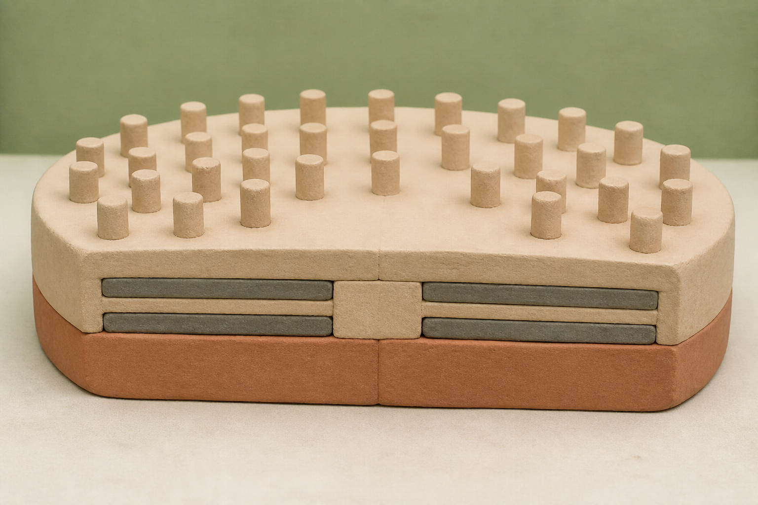
What changes in this design
A person might expect separate electrical pieces to be placed directly between two sheets, leaving empty gaps around the raised parts.
Rather than leaving empty spaces, this technique fills the gaps with an insulating material until the surface is level with the electrode pieces, then bonds a second sheet across that flat top.
Creating a level foundation makes it possible to attach the final upper sheet securely across both the electrical components and the spaces between them.
The speed trap of High-NA optics
The push to print eight-nanometer transistor features comes with an uncomfortable mechanical penalty. In ASML's High-NA EUV platform, the TWINSCAN EXE:5000, specialized anamorphic projection optics shrink circuit patterns by 1.7 times compared to earlier machines, yielding nearly triple the transistor density. But shrinking those images halves the exposure field size on the wafer. To keep the tool running at 110 wafers per hour, the wafer stage cannot move at its old pace. It has to accelerate across the exposure slit with unprecedented speed.
When we look at the mechanics of shrinking transistors down to eight nanometers, the light source usually gets all the attention. The physical reality underneath the wafer is much grittier. Accelerating a 300-millimeter silicon disc back and forth dozens of times a second creates immense inertial and thermal stress. If the wafer slips by even a fraction of a nanometer, the entire layer is ruined.
Clamping silicon without air
Holding a wafer flat sounds simple until you remember where extreme ultraviolet lithography takes place. Because 13.5-nanometer light is readily absorbed by ordinary atmospheric gases, the entire exposure happens inside a high-vacuum chamber. Standard vacuum chucks, which hold objects by creating suction against atmospheric air pressure, cannot function at all.
The only practical solution is electrostatic clamping. The tool applies between one and eight kilovolts to embedded electrodes, creating an electric field that pulls the silicon wafer down against an array of microscopic burls. Those tiny studs minimize contact area to prevent stray dust particles from distorting the wafer, while also conducting away heat. As early as 2003, patent filings established strict operating boundaries for these chucks, requiring dielectric materials with volume resistivity above 10^16 Ohm-centimeters and near-zero thermal expansion to balance electrical release speed against structural stability.
The flaw in glued layers
For years, chuck manufacturing relied on thin-film layers and adhesives. In a 2021 patent, ASML described an object holder architecture where an electrostatic sheet with embedded electrodes was glued to a core body with an adhesive layer at least 100 nanometers thick. Earlier designs from 2012 and 2013 tried depositing dielectric material into etched electrode gaps, but struggled with parasitic capacitance and non-uniform electrostatic fields.
If we compare this to the company's 2021 object holder design, the difference in philosophy is stark. Glue is easy to apply, but high vacuum and multi-kilovolt fields punish organic bonds. Over millions of exposure cycles, adhesive interfaces degrade thermally and develop microscopic voids. Under four or five thousand volts, any tiny void inside the dielectric can trigger an electrical arc, destroying the clamp.
Diamond electrodes and nine hundred degrees
ASML's published patent application, US20260259512A1, filed by inventor Volker Schmidt, proposes rebuilding the electrostatic electrode from the ground up for 340 mm to 400 mm wafer holders. Instead of laminating sheets with glue, the method forms a monolithic, void-free ceramic sandwich.
The process starts by depositing conductive electrode portions on an insulating base. These electrodes are made from exceptionally hard materials exceeding 9 GPa on the Vickers scale, such as titanium nitride or boron-doped diamond containing 100 to 8,000 parts per million boron. After etching gaps of at least 0.1 millimeters between the electrode segments, the spaces are backfilled with a softer dielectric insulator and polished into a continuous planar surface.
Then comes the assembly. A second insulating layer of silicon nitride, aluminum oxide, or aluminum nitride is placed directly onto the planar surface and diffusion bonded at temperatures between 240°C and 2,000°C - ideally around 900°C - under pressures between 50 and 2,000 bar. The detail that caught my eye in the published record is the sheer violence of the bonding step. Applying 500 bar of pressure at near-melting temperatures forces the ceramic layers to fuse at the atomic level, squeezing out every microscopic gas pocket.
What the filing is really betting on
I doubt most chipmakers expected electrostatic clamps to require synthetic diamond and furnace diffusion, but the mechanical math leaves little choice. The filing is betting that only a completely void-free ceramic electrode can survive the kilovolt clamping forces and rapid thermal shifts of High-NA lithography without arcing or drifting.
What I find most telling is that a mechanical clamp, no matter how flawless, cannot solve wafer positioning errors entirely on its own. Even with a void-free ceramic clamp, we know from earlier research that intense localized radiation causes dynamic thermo-mechanical distortions across the substrate. A hot beam striking silicon will always cause uneven expansion that requires real-time mathematical modeling to correct.
Still, software compensation needs a predictable physical baseline to work. By welding ceramics and diamond into a single solid block, the filing eliminates the creeping degradation of adhesives and microscopic voids. It is an unglamorous manufacturing upgrade, but without it, the fastest stages in the semiconductor industry would literally lose their grip.
Sources
Reporting for this piece drew on the published filing and the references below.
- Method Of Manufacturing An Electrode For An Object Holder - Justia Patents
- EP4481491A1 - Method of manufacturing an electrode for an object holder - Google Patents
- TWINSCAN EXE:5000 - EUV lithography systems | ASML
- EUV lithography - Wikipedia
- WO2021185552A1 - Object holder, tool and method of manufacturing an object holder - Google Patents
- EP2555234A2 - Electrostatic clamp, lithographic apparatus and method of manufacturing an electrostatic clamp - Google Patents
- WO2013156236A1 - Substrate holder, lithographic apparatus, and device manufacturing method - Google Patents
- US6864957B2 - Chuck, lithographic projection apparatus, method of manufacturing a chuck and device manufacturing method - Google Patents
- US10564555B2 - Method of reducing effects of reticle heating and/or cooling in a lithographic process - Google Patents
The record, briefly. US20260259512A1, “Method Of Manufacturing An Electrode For An Object Holder” A method of manufacturing an object holder electrode involves forming spaced electrode portions on a first insulating layer, forming an insulating portion between them to fill the space and establish a planar surface with the electrode portions, and bonding a second insulating layer to the planar surface.
More angles on this
- CPC G03F: Photomechanical production of textured or patterned surfaces, e.g. for printing, for processing of semiconductor devicesThe official classification family this record was filed into, published in the USPTO Cooperative Patent Classification scheme.
- Camera Array With Reduced Cross-Talk Makes the Next Move Easier to SeeAnother reading from the neighbouring G03B classification family, apparatus or arrangements for taking photographs or for projecting or viewing them.
- Portable And Low-Cost Microscopic Imaging Device Makes a Small Case for Better TimingAnother reading from the wider G02B classification family, optical elements, systems or apparatus.
- When Angled Light Takes the HandoffAnother reading in the same Field Notes category on this site.
Read around this one:Public patent recordUSPTO published figure