Objects
Semiconductor Device And Method Of Manufacturing The Same Makes the Next Move Easier to See
As 3D flash memory stacks climb past two hundred layers, chipmakers are running out of optical headroom to keep microscopic holes lined up from top to bottom.

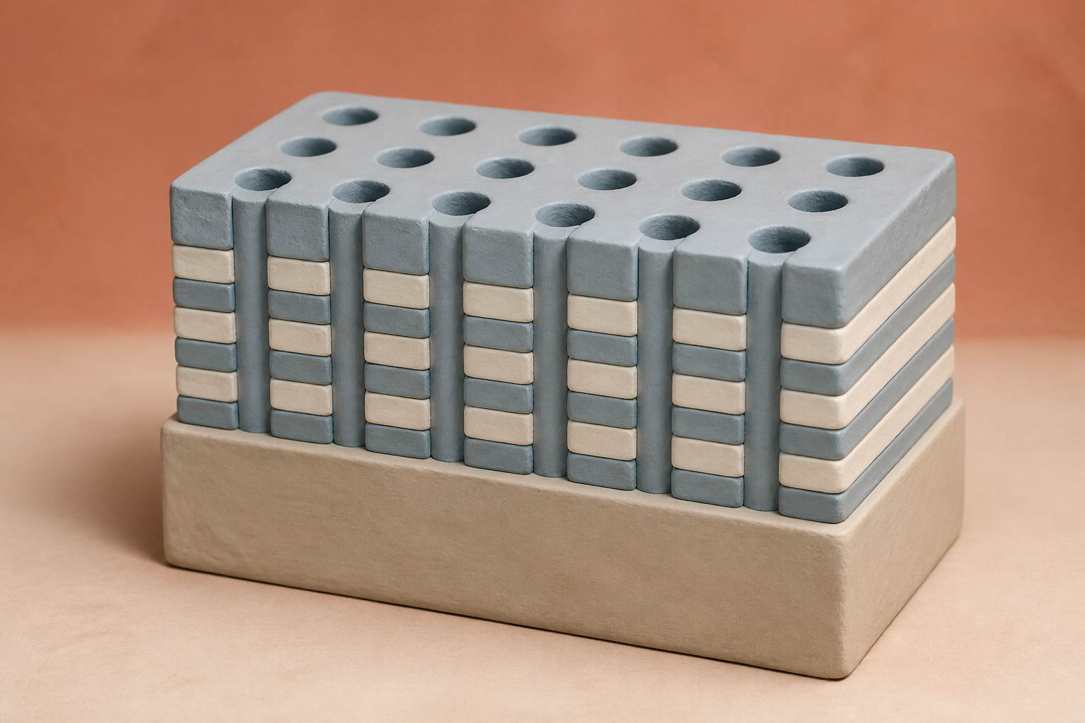
What changes in this design
Layered electronic components often bounce significant amounts of light off their upper surfaces. When light scatters across stacked materials that have varying optical qualities, tracking internal alignment holes becomes difficult.
Here, a dedicated anti-reflective coating sits directly on the stack with pre-aligned holes matching the openings underneath. That top layer actively limits light reflectance to 25 percent or less.
Controlling surface reflection at twenty-five percent or lower ensures light bounce is significantly contained across these drilled, multi-layered assemblies.
The twenty-four layer bet
On August 8, 2013, Samsung announced that its Hwaseong fab had begun mass production of the world's first three-dimensional flash memory, a 128-gigabit chip built with 24 layers of memory cells. At the time, industry analysts questioned whether stacking memory gates like floors in a high-rise was a sustainable manufacturing path or a costly one-off experiment. Planar flash had hit its physical scaling limits, and going vertical felt like an extraordinary gamble. When we look back at that 2013 announcement, the scale of the mechanical shift becomes clear.
Today, commercial chips regularly top 230 layers, and Samsung has floated targets of 1,000 layers by 2030. But building taller towers introduces a relentless physical problem: connecting all those tiers requires etching millions of microscopic channel holes straight down through the entire stack. When a chip was 24 layers tall, etching through the alternating layers was relatively straightforward. Today, a 232-layer part from YMTC features a vertical channel height of 12.4 microns, compared to 8.9 microns for a 176-layer generation from Samsung with a 43-nanometer word-line pitch. Drilling a channel under 100 nanometers wide through ten vertical microns of alternating materials is an extreme exercise in precision.
A one-nanometer margin for error
Because etching a single continuous hole through hundreds of layers causes structural defects, chipmakers build their stacks in multiple tiers. They deposit dozens of alternating oxide and nitride layers, etch the bottom holes, deposit the next tier on top, and etch again. The catch is that the upper channel hole must land squarely on top of the lower one.
The number that caught my attention in the engineering reports was 150 square nanometers. In a modeled two-tier stack containing 64 oxide-nitride layers in each tier, a tilt of just one nanometer in the lower hole costs roughly 150 square nanometers of contact area between tiers. If that overlap shrinks too far, the channel cannot punch through to the source line, destroying the entire die.
Every major memory maker has spent years patenting ways to manage this alignment nightmare. SK Hynix patented an approach in US9911751B2, developed by inventors Woo June Kwon, Jong Hoon Kim, and Chan Sun Hyun, that etched tier-by-tier and used a reflective metal pattern as both an etch-stop layer and an overlay-measurement mark. An American competitor targeted the same problem in US11276569, patenting methods to correct in-plane distortion and lithographic overlay errors across tiers. What we are seeing is an industry fighting the same stubborn geometry from every available angle.
Reflections inside a deep canyon
A newly published patent application, US20260259351A1, titled "Semiconductor Device And Method Of Manufacturing The Same," extends this direct lineage with a different optical tactic. It describes a substrate supporting a stacked structure of alternating material layers with differing refractive indices, pierced by vertical through-holes. Embedded in this stack is an anti-reflective layer with pattern holes aligned with the through-holes, exhibiting a light reflectance of 25% or less.
To understand why low reflectance matters, consider how factory equipment inspects these microscopic shafts. Most fabrication lines use infrared optical metrology because optical systems are fast enough to keep pace with factory throughput. But when light travels down a channel less than 100 nanometers wide and ten microns deep, the alternating dielectric layers create intense optical interference. Light bounces off internal boundaries with differing refractive indices, scattering the signal. By adding an anti-reflective layer with reflectance at or below 25%, the filing seeks to suppress stray reflections, sharpening the optical signal so lithography tools can align the next tier accurately.
The limits of looking down
I doubt optical inspection can stretch much further before hitting a hard physical barrier. At depths between six and ten microns, standard infrared metrology loses spectral resolution and reliability because the material absorbs the optical signal. The reflected light simply carries too much noise to yield dependable overlay measurements.
There is an alternative method: critical-dimension small-angle X-ray scattering, or CD-SAXS. X-ray tools can measure tier-to-tier tilt and overlay far more accurately because X-rays slice through thick stacks without optical signal loss. But X-ray tools cannot compete with optical equipment on throughput. A high-volume fab cannot afford to pause its line while an X-ray tool scans individual test sites. Chipmakers remain tethered to optical metrology, patching its blind spots with specialized anti-reflective layers and pattern holes.
Where this leaves things
I suspect the industry is reaching the point where etching taller single-stack towers no longer makes economic sense. Etch speeds cannot simply be accelerated, and adding more layers has become less efficient at reducing manufacturing costs when alignment margins are measured in single nanometers.
Instead of trying to drill deeper, alternative manufacturing strategies are attempting to bypass the problem. YMTC has been aggressively securing patents on hybrid bonding, building two separate dies with shorter, more manageable layer counts and bonding them face-to-face to reach 400 layers and beyond. That method eliminates the need to etch one continuous, flawless channel hole through an impossibly tall monolithic stack.
The published filing represents the continuous refinement of an established approach: build taller, drill deeper, and use optical coatings to help sensors verify where the holes went. Whether that strategy can survive all the way to 1,000 layers remains our central open question.
Sources
Reporting for this piece drew on the published filing and the references below.
- Semiconductor Device And Method Of Manufacturing The Same (US20260259351A1)
- Manufacturing method for semiconductor device having hole penetrating stack structure (US9911751B2)
- On stack overlay improvement for 3D NAND (US11276569)
- Comparison: Latest 3D NAND Products from YMTC, Samsung, SK hynix and Micron
- Is There A Limit To The Number of Layers In 3D-NAND?
- The Impact Of Channel Hole Profiles On Advanced 3D NAND Structures
- Metrology Digs Deep To Produce Next-Generation 3D NAND
- YMTC's hybrid bonding patents: is Samsung losing ground in 400+ layer 3D NAND?
The record, briefly. US20260259351A1, “Semiconductor Device And Method Of Manufacturing The Same” The semiconductor device includes a substrate, a stacked structure of alternating material layers with differing refractive indices and through holes extending through them, and an anti-reflective layer with pattern holes aligned with the through holes and having a light reflectance of 25% or less.
More angles on this
- Inside chain-type metamaterial absorberAnother reading from the same G02B classification family, optical elements, systems or apparatus.
- Inside protective film, methodAnother reading from the same G02B classification family, optical elements, systems or apparatus.
- CPC G02B: Optical elements, systems or apparatusThe official classification family this record was filed into, published in the USPTO Cooperative Patent Classification scheme.
- CPC H10W: Generic packages, interconnections, connectors or other constructional details of devices covered by class H10The official classification family this record was filed into, published in the USPTO Cooperative Patent Classification scheme.
- Photon Detection Marks a Pause Worth NoticingAnother reading from the neighbouring H10N classification family, electric solid-state devices not otherwise provided for.
Read around this one:Public patent recordUSPTO published figure