Objects
A Memory Device That Treats the Edge as a Place to Think
The company now called Kioxia showed the world how to stack memory chips in 2007, and its latest patent claims a tiny engineered gap in a market where it runs third.

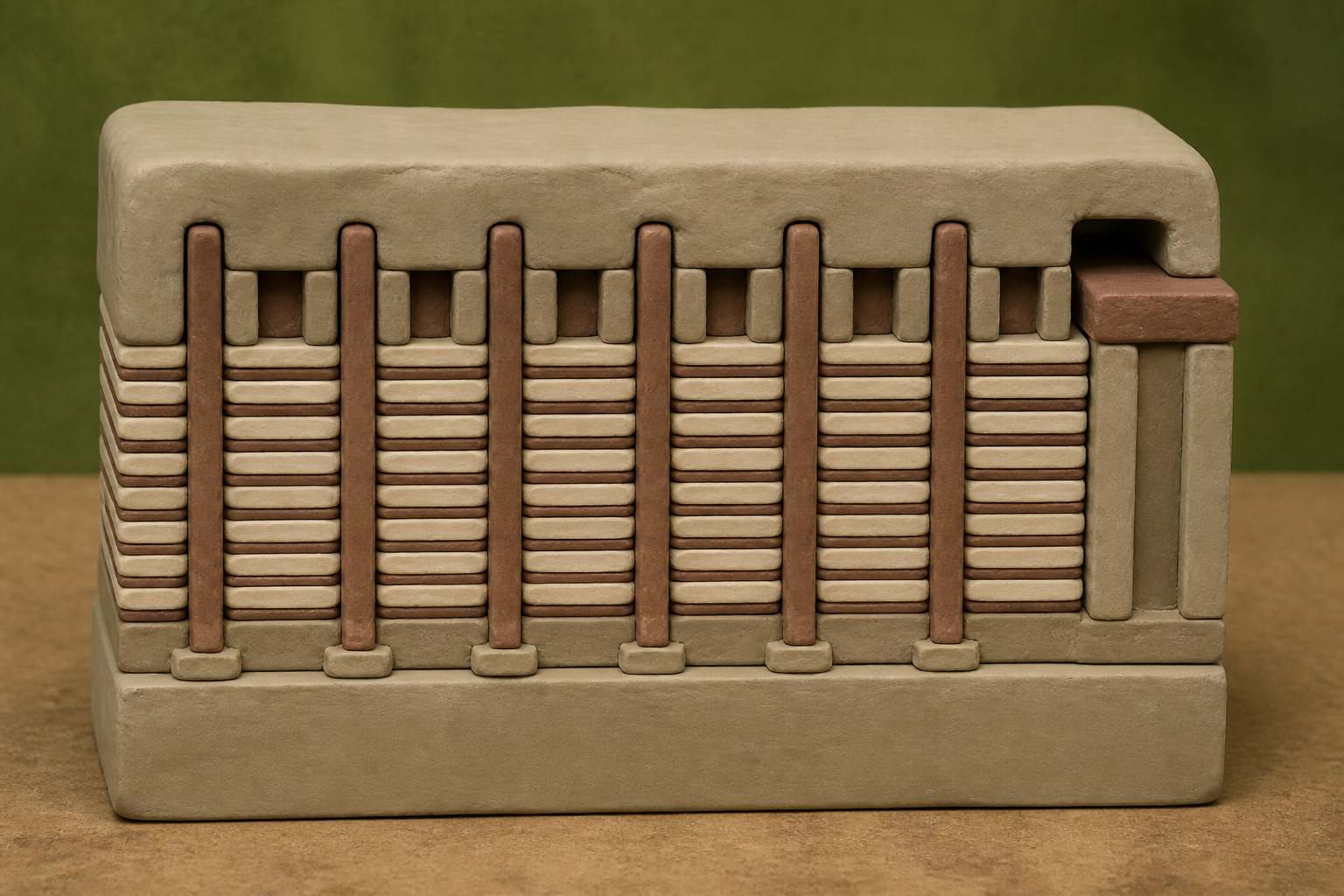
What changes in this design
Someone may picture a memory component simply as a small electronic part that holds information. How such components are ordinarily built is not stated.
Here, the component includes alternating conductive and insulating sheets, plus a pillar with a semiconductor strip that rises above them. It also has a nearby plate-like piece with a projecting conductive strip, a semiconductor-containing cover, and an empty space at the piece's upper end.
These details give a physical picture of the device's build rather than treating it as an unseen box. What they change or measure is not stated.
The announcement came in 2007
In 2007, engineers from the memory arm of a large Japanese electronics company stood up at a technical conference and told their industry where flash memory had to go: up. Flat chips were running out of room to shrink. The answer was vertical: stack the cells in towers, layer on layer.
The idea was right; the timing was wrong. A Korean rival shipped the first commercial version in 2013. By the fourth quarter of 2025 the market leader held 28 percent of NAND revenue, a second Korean rival 22.1, and the company that had announced the concept first, 15.6. It's now called Kioxia. When it listed in Tokyo in December 2024 it was valued at a little over five billion dollars. A fine number for most companies. A strange one for the firm that first described the architecture underneath modern storage.
A void, on purpose
The filing I read was published as US20260253622A1, lists Kioxia as applicant, and traces its priority to a Japanese application filed on February 25, 2025. It claims a 3D memory device: alternating layers of conductor and insulator, a pillar of memory material poking above the stack, a plate-like contact beside it, a covering layer over it all. And one more feature: a void, left at the upper end of the plate-like contact. Nothing in a device like this is accidental.
These chips are built to extraordinary precision. Kioxia's generation in production stacks 218 word lines in one tower; the next, sampling this summer, reaches 332. But the straightforward path, adding more floors, is closing. SK hynix cut its 2026 target to 375 layers and is swapping the metal in its word lines from tungsten to molybdenum. The cheap trick got expensive.
The industry is changing its answer. Instead of etching ever taller towers, the big makers build wafers separately and bond them together. Kioxia calls its version CBA, CMOS directly bonded to array; the market leader showed a working 900-layer prototype this May by bonding two 450-layer wafers.
The rival on the share register
Now the uncomfortable part of Kioxia's corporate life. SK hynix, the rival that beats it in memory, is also one of its largest shareholders, through the buyout consortium that carved it out of its former parent. SK hynix holds about 19 percent of that consortium, convertible bonds could lift its ownership to roughly a third, and its voting rights stay capped at 15 percent through 2028.
The arrangement has teeth. When Kioxia tried to merge with an American storage maker, SK hynix blocked it. The two companies say no business discussions are underway between them. A rival holds a slice of the company and has already used its seat to kill a deal.
The shortage, then the glut
The market has been whipping around beneath all of this. In September 2025, an AI-driven NAND shortage sent Kioxia's stock up 70 percent in a month. By November, its quarterly profit had fallen 62 percent from the year before, a second steep drop. Analysts who track memory prices already describe the next turn: contract prices start falling in the third quarter of 2027, swinging from a 10.8 percent supply deficit in early 2026 to a 12.2 percent surplus by late 2027, as new plants, Kioxia's K2 fab among them, come online. Memory stocks sat about 30 percent below their May peak by late July. The cycle is familiar. It still lands hard.
The Japanese state has skin in this too. The industry ministry has committed up to 243 billion yen toward a 729 billion yen co-investment in 218-layer production, part of a push to triple domestic chip sales.
Where the risk actually sits
Which brings me back to the void. I can't tell you from the public record what job the gap performs. Patent prose says what, not why. But it's the kind of detail that decides real money: a small change in how a contact is formed can be the difference between a chip that yields well and one that doesn't, and yield is the whole game when you hold 15.6 percent of a market with two rivals above you.
The easy story here is a company that lost the lead it created. I don't think that's the interesting one. The firm that announced 3D memory in 2007 kept inventing. Its strongest rival owns a capped stake in it and blocked its merger. Its government is underwriting its factories. This filing, a gap engineered into a stacked memory chip, is one small patent inside that survival bet. The risk isn't whether Kioxia can keep thinking of things like engineered voids. It's whether the market will pay enough for flash, in 2027, to make the thinking matter.
Sources
Reporting for this piece drew on the published filing and the references below.
- US20260253622A1 - Semiconductor Memory Device And Method For Manufacturing Semiconductor Memory Device
- V-NAND - Wikipedia
- Samsung tests 900-layer NAND prototype to reclaim market lead - Edgen
- Overview of new technologies applied to BiCS FLASH generation 8 - Kioxia
- The Race to 400-Layer NAND - TrendForce
- Kioxia - once Toshiba's chip unit - rallies after a Tokyo debut - Fortune
- Kioxia's Post-Earnings Challenges - TrendForce
- Kioxia Stock Jumps 70% on NAND Shortage - TrendForce
- Japan stumps up more cash for Kioxia and WD memory venture - The Register
The record, briefly. US20260253622A1, “Semiconductor Memory Device And Method For Manufacturing Semiconductor Memory Device” The semiconductor memory device includes alternating first conductive and insulating layers, a pillar with a semiconductor layer projecting above the stacked body, an adjacent plate-like portion with a projecting second conductive layer, a semiconductor-containing covering first layer, and a void at the plate-like portion's upper end.
More angles on this
- A Sideways Reading of Split StaircasesAnother reading from the same G11C classification family, static stores.
- CPC G11C: Static storesThe official classification family this record was filed into, published in the USPTO Cooperative Patent Classification scheme.
- CPC H10B: Electronic memory devicesThe official classification family this record was filed into, published in the USPTO Cooperative Patent Classification scheme.
- Liquid Cooling Heat Dissipation Device For Multi-Disk Drive System Marks a Pause Worth NoticingAnother reading from the neighbouring G11B classification family, information storage based on relative movement between record carrier and transducer.
- The Clip Needs Its ContextAnother reading from the wider H04N classification family, pictorial communication, e.g. television.
Read around this one:Public patent recordUSPTO published figure