Objects
A Sideways Reading of Split Staircases
Flash chips stopped being one tall stack years ago, and every deck now pays its own staircase tax in die area - which is what this filing is really about.

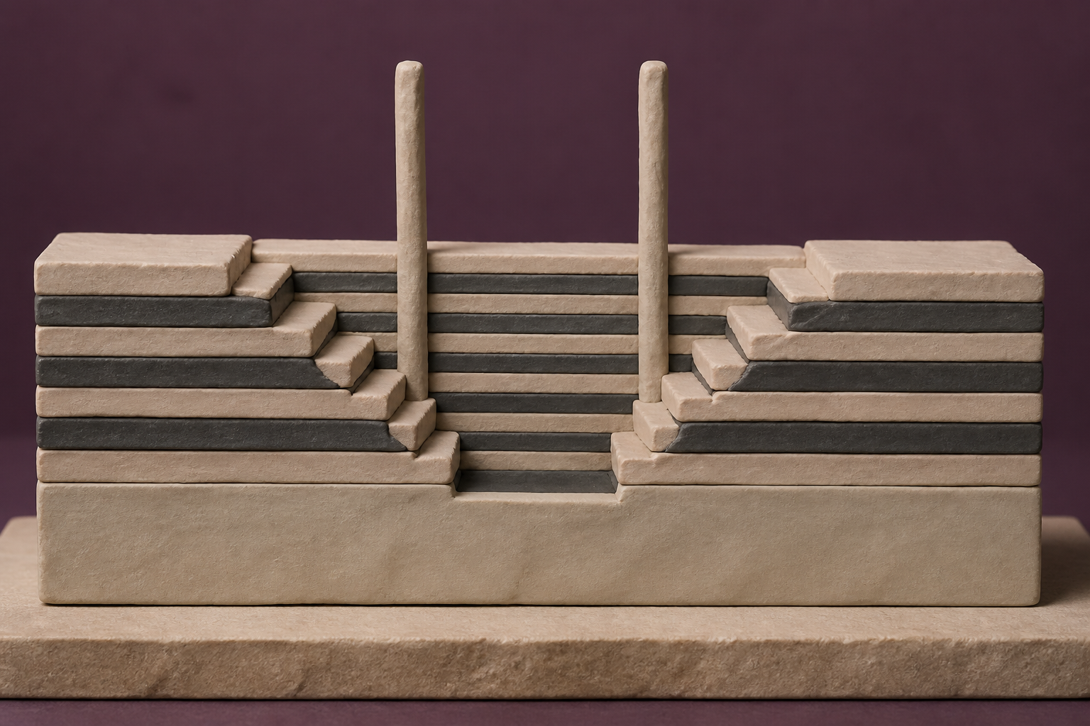
What changes in this design
A reader might picture each stepped insulating area as one continuous piece rather than a group separated across the width of the device.
Here, each of the first, second, and third levels has alternating insulating and electrically conductive layers with stepped dielectric portions inside. In at least one set, three or more of those portions are spaced sideways from one another.
The key visual idea is not only stacking layers upward. It also splits at least one group of stepped insulating pieces across the width, which gives the title's laterally split staircases a concrete meaning.
A staircase measured in micrometres
Cut open a 3D flash chip and you will find a staircase. It isn't decorative. Every conductive layer in the stack has to be reached by a contact dropped in from above, so the layers get cut back one at a time into steps. Teardown work presented at a 2018 industry conference put a number on what that costs: on one 64-layer part, the staircase took 0.82% of the die, and that was after a 45% width reduction from the generation before.
I think that sounds small until you look at what the rest of the die is doing. One critical reading of the technology found that memory cells occupy only about 40% of a 3D die, against more than 65% on the older planar parts it replaced, and that at 32 layers the word line staircase already ran about 20 micrometres at the edge of the cell array. Those figures belong to the early years of 3D flash. The problem they name has not gone away.
Nobody builds one tall stack anymore
Somewhere along the way the industry stopped stacking. Not literally, since the layer counts keep climbing, but the tall single column quietly became an assembly. A Korean manufacturer reached 321 layers in November 2024 by stringing three 100-plus-layer stacks together. The 332-layer part that began sampling in July 2026 is built the same way: three decks rather than one column, carrying a 1Tbit die.
Samsung went further in May 2026 with a working 900-layer research die, built as two 450-layer decks. Getting there needed a new chuck design to control wafer warpage and new overlay correction to keep the decks aligned. Here is the part that matters, in my view: every deck needs its own staircase. Triple the decks and you triple the tax, unless you change the shape of the staircase itself.
Five days after the spin-off
On 21 February 2025 a large storage company completed the separation of its hard drive and flash businesses into two independent firms. The day before, the flash side and its Japanese manufacturing partner had publicly previewed that 332-layer design. Five days after the separation closed, on 26 February 2025, SanDisk filed application 19/064385. It published on 27 August 2026.
The filing describes first, second and third tier structures, each an alternating stack of insulating and conductive layers with retro-stepped dielectric portions embedded in them, and at least one set where three or more of those portions sit laterally spaced apart. Put plainly: three decks, and at least one deck's staircase broken into three or more pieces placed side by side. The background section reaches back to a 2001 conference paper on stacked surrounding-gate cells. A 2025 filing anchoring itself to a 24-year-old idea isn't unusual, but it is telling, I think.
Two granted patents got there first
The idea of splitting a staircase sideways was not new in 2025. YMTC, the Chinese flash maker, was granted a patent in October 2022, on an application from May 2019, covering staircases divided into offset blocks so the number of steps running parallel to the word lines could be greatly reduced. A second one, granted in June 2022 from a 2020 filing, patterns several sub-staircase regions and then overlays a second structure to multiply the step count.
The motivations differ. Those earlier patents talk about lateral dimension, and about the cost and low throughput of the repeated trim-and-etch cycles that carve steps one at a time. They also name a failure mode I hadn't considered: contact holes on the lower staircase levels can come out much wider than the ones at the top. Whether any specific claim overlaps is an examiner's question, not mine. But laterally subdivided staircases were public, granted art five and six years before this application.
One more thing sits under all of this. In December 2022, US export controls on flash manufacturing tools were drawn at a threshold of 128 layers or more, and the Commerce Department was preparing to move YMTC onto its Entity List. The threshold is counted in layers. The thing being counted has since become an assembly of decks, and the decks in the newest three-deck parts run a hundred-odd layers each. I don't know what regulators make of that.
What the filing is really betting on
So what is the bet? It isn't, to my mind, that splitting a staircase is clever - two granted patents from a rival say otherwise. The bet is that deck count keeps rising, that every new deck arrives with its own area penalty, and that owning the geometry of how those staircases are carved and placed is worth something for the next decade. Read that way, the filing is less an invention than a dated core sample. A company on its fifth day of independence, staking ground on the one part of the chip that refuses to shrink.
Sources
Reporting for this piece drew on the published filing and the references below.
- Western Digital Corp Form 10-K FY2025 (SEC EDGAR)
- Kioxia, SanDisk tease 332-layer 3D NAND future (Blocks & Files)
- Kioxia and SanDisk sample shipping 332-layer 3D NAND (Blocks & Files)
- Samsung opens door to 900-layer 3D NAND (Blocks & Files)
- TechInsights memory technology update from IEDM18
- US11462558B2 - Staircase structure with multiple divisions for three-dimensional memory
- US11361988B2 - Staircase formation in three-dimensional memory device
- US to slap trade restrictions on China's YMTC (Blocks & Files)
The record, briefly. US20260253619A1, “Three-Dimensional Memory Device Containing Laterally Split Staircase Regions” A device structure has first-, second-, and third-tier structures, each with alternating insulating and electrically conductive layers embedding retro-stepped dielectric material portions; at least one set has three or more portions laterally spaced apart.
More angles on this
- The Useful Quiet Room Beside MemoryAnother reading of a record filed by the same applicant, Sandisk Technologies.
- When a Pair Does Not MatchAnother reading in the same Objects category on this site.
- What Holds the SpaceAnother reading of a record filed by the same applicant, Sandisk Technologies.
- A Memory Device That Treats the Edge as a Place to ThinkAnother reading in the same Objects category on this site.
- Half Width Is Not the Whole QuestionAnother reading in the same Objects category on this site.
Read around this one:Public patent recordUSPTO published figure