Objects
What Holds the Space
Flash memory sells on layer count, but this year the taller stack lost - and a new Sandisk filing is about holding the stack still, not making it higher.

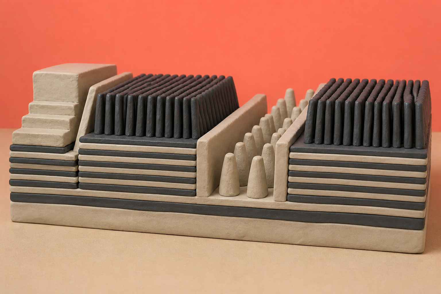
What changes in this design
Someone might picture a memory chip as a flat layout with a single wall between adjacent areas. That picture leaves out the upward stack of many layers and the extra insulating pieces that can sit with a wall.
Here, two memory areas lie side by side, each holding a multi-level stack that alternates insulating and conductive layers. Filled holes run through the stacks. The divider between the areas may combine wall-like insulating sections with upright pillars or stepped insulating portions.
For someone trying to picture the chip, the point is that the divider can be more than a wall. The record does not identify a performance outcome from the alternative pieces.
A hundred trillion holes in one wafer
The number that stopped me was a hundred trillion. That is roughly how many memory holes may be etched into a single 300mm wafer of 3D flash memory, the storage in your phone and the drive under your desk. Each hole runs about 100 nanometres wide and five to six micrometres deep. At 128 layers that is an aspect ratio near 50 or 60 to one, and getting to a thousand layers would need better than 100 to one.
Think about what that does to a piece of silicon. You drill a block until it is mostly absence, then refill the holes with materials that each expand and contract on their own schedule. The tooling is extraordinary: one equipment supplier counts more than 7,500 high-aspect-ratio etch chambers in production and over 100 million NAND wafers processed, with cryogenic etch running 2.5 times faster and twice as precise on profile. Nobody puts the flatness problem on a product page.
332 layers against more than 400
Layers are what gets marketed. It is one clean number, it goes up every year, and it is the one figure a reader remembers. This year it stopped meaning what people assume.
Kioxia's tenth-generation BiCS flash, co-developed with Sandisk, is 332 layers. It reaches over 29 gigabits per square millimetre in three-bit cells and over 37 in four-bit. Samsung's competing part clears 400 layers. On density per square millimetre the shorter stack holds its own, and the improvements the 332-layer part claims over the eighth generation - 59% more bit density, a 33% faster interface, 30% better read power - are credited to bonding the CMOS control wafer directly onto the array wafer and to a redesigned select gate. Not to height. A third large maker quietly cut its own 400-layer goal to 375 for the end of 2026. Vertical is getting expensive, and everyone has found a sideways route.
A filing dated five days after independence
Which is what makes the filing I want to show you interesting. On 26 February 2025, Sandisk filed application 19/064464. It published on 27 August 2026 as US 2026/0253621 A1, under the title Three-Dimensional Memory Device Containing Dielectric Structural Support Elements Between Dielectric Wall Structures.
Strip the language and it describes scaffolding. The device has stacks of alternating insulating and conductive layers, split into two memory array regions with a gap between them, and memory holes filled through those stacks. In the isolation regions that separate everything, the claim puts dielectric support elements - pillars, or retro-stepped dielectric portions - between the dielectric walls, so a continuous barrier runs from the first array region, across the region between, into the second. It adds no capacity. It does not shrink a cell. Its stated purpose is keeping the structure stable as stacks get taller.
The date matters. Five days earlier, the company had completed its separation from the disk drive maker it had belonged to, becoming an independent listed business. Whatever else that week involved, the research did not stop.
The same problem, worked since 2021
This is not a new idea arriving. The same company, under its former parent, filed in September 2021 on perforated wall supports for the same inter-array region, with lateral openings at the insulating levels so sacrificial material could be etched out while the wall kept bracing the stack. That one issued in April 2024. The 2026 filing is the next turn of a problem the engineers have had on their desk for at least four years, which is usually a sign the problem is real rather than speculative.
There is one more thing I would not have guessed. The company that owns this patent does not own a fab that can make it alone. Its flash is built in joint ventures with Kioxia, and in January 2026 the two extended those ventures from 2029 to 2034, with Sandisk paying about $1.165 billion for manufacturing services across 2026 to 2029. They compete for the same customers and share the same buildings.
The part worth watching
I think the honest reading is that this filing defends an axis the industry is partly routing around. Bonding the logic wafer to the array wafer, better lateral packing, cryogenic etch - those are where this year's density came from, and all three big makers arrived at bonding separately. A patent on internal bracing is insurance for the case where stacks keep climbing anyway.
What I would watch is whether it gets asserted rather than used. Structural 3D flash patents are already being litigated: a Chinese maker has sued a US one over 11 patents covering 96 to 232-layer parts. Scaffolding is unglamorous, and unglamorous claims are the ones that turn out to be unavoidable.
Sources
Reporting for this piece drew on the published filing and the references below.
- Three-dimensional memory device with dielectric or semiconductor wall support structures (US 11,963,354 B2)
- Western Digital Form 8-K: completion of the Sandisk spin-off
- Kioxia and Sandisk Extend Yokkaichi Joint Venture Agreement Through 2034
- Kioxia Commences Sample Shipments of 10th-Generation BiCS FLASH Devices
- The Race to 400-Layer NAND: Roadmaps and Key Technologies Driving Samsung, SK hynix, and Kioxia
- How Etch Breakthroughs Are Tackling 3D NAND Scaling Challenges on the Path to 1,000 Layers
- China-US Chip War Escalated as YMTC Sues Micron for Patent Infringement
The record, briefly. US20260253621A1, “Three-Dimensional Memory Device Containing Dielectric Structural Support Elements Between Dielectric Wall Structures And Methods For Forming The Same” A semiconductor structure has laterally separated multi-tier stacks of alternating insulating and conductive layers, memory-opening fill structures through stacks in two memory array regions, and lateral isolation structures that may combine dielectric walls with pillar or retro-stepped dielectric portions.
More angles on this
- A Sideways Reading of Split StaircasesAnother reading from the same G11C classification family, static stores.
- CPC G11C: Static storesThe official classification family this record was filed into, published in the USPTO Cooperative Patent Classification scheme.
- CPC H10B: Electronic memory devicesThe official classification family this record was filed into, published in the USPTO Cooperative Patent Classification scheme.
- Liquid Cooling Heat Dissipation Device For Multi-Disk Drive System Marks a Pause Worth NoticingAnother reading from the neighbouring G11B classification family, information storage based on relative movement between record carrier and transducer.
- The Clip Needs Its ContextAnother reading from the wider H04N classification family, pictorial communication, e.g. television.
Read around this one:Public patent recordUSPTO published figure