Objects
Half Width Is Not the Whole Question
Intel got out of making memory but never stopped inventing it, and one quietly reassigned filing shows where that invention ends up.

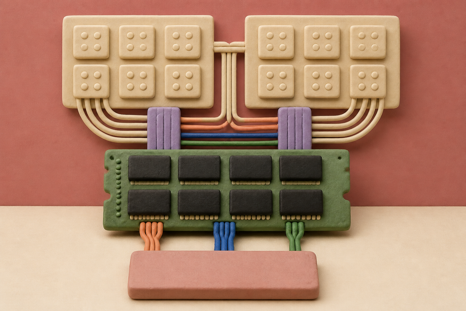
What changes in this design
A reader might assume that half-width operation has a single fixed way of reaching the memory banks. This record gives no information about how other DRAM devices are ordinarily set up.
This record lays out two half-width modes. In one, a single narrower route reaches all banks. In the other, two independent sets of data wires each reach its own portion of the banks.
This matters because the phrase half-width alone does not tell a reader which bank-access pattern is being used. The record distinguishes a single route to all banks from two independent routes to portions.
Half the chips, left off on purpose, since 2021
In late 2021, people chasing DDR5 frequency records found a trick that needed no new silicon. Populate only one of a module's two 32-bit sub-channels, leave the other half of the chips off, and the memory trains at speeds it will not reach fully loaded. The technique held across three generations of one vendor's desktop platforms. It isn't a hack the standards missed, either: the presence-detect spec already has a field for single sub-channel modules.
The cost isn't small. A recent analysis of these modules puts throughput degradation at 40 to 60 percent in bandwidth-bound workloads, under 10 percent when latency dominates. It also documents an inversion that should bother anyone buying on the number on the box: DDR5-4800 running one sub-channel falls below DDR4-3200. It doesn't work everywhere, either: one rival desktop platform trains memory as a unified 64-bit unit.
Thirty-two banks and twelve data lines
So half width is old. A filing published on August 27 this year proposes doing it properly, inside the DRAM die. It sets out two modes: one where a single partial channel reaches every bank on the die, and one where two independent half-width buses each own a portion of the banks. The lead drawing is an LPDDR6 die: eight bank groups of four banks, thirty-two in all, split into Partial Channel 0 on twelve data lines and Partial Channel 1 on the other twelve, each with its own command bus. The title says the quiet part, doubling of bank resources. Half the width, all the banks.
The part that pulled me in is the front page. Sole inventor, Kuljit S. Bains of Olympia, Washington. Application 19/652,288, filed April 20, 2026, expressly a continuation of application 17/944,980 from September 14, 2022. Same title, same abstract, same classification codes, same inventor. The 2022 parent lists Intel Corporation as applicant. The 2026 child lists Intel Products IP LLC as both applicant and assignee. The disclosure didn't change. The name holding it did.
What JEDEC published on July 9, 2025
Between those two dates, the standard arrived. JEDEC published LPDDR6 on July 9, 2025: two sub-channels per die, twelve data lines each, 32-byte access granularity. It includes a static efficiency mode for high-capacity configurations, described as maximizing bank resource utilization - close enough to the filing's title to read twice - and a dynamic efficiency mode for single sub-channel low-power operation. The shift that makes any of this matter: a 24-bit channel split into two 12-bit halves, where LPDDR5 had 16 bits and no split at all.
SK Hynix's numbers at ISSCC
At this year's ISSCC, SK Hynix presented a 16-gigabit LPDDR6 die on a 1-nanometer-class process: 14.4 gigabits per second per pin, 38.4 gigabytes per second per die. In single sub-channel operation at 12.8 Gbps, standby current dropped to 87.3 percent of normal and operating current to 81.1 percent. Half width isn't a proposal any more. It runs, and the saving is real but modest: about a fifth off operating current for half the bus.
Row hammer, and what a standard doesn't prove
Bains is not a marginal figure. He is first-named inventor on the 2012 application that became the targeted refresh patent, describing a controller that detects a row hammer event and refreshes the adjacent victim row. That mechanism became Target Row Refresh, written into DRAM standards the entire industry ships.
Then in 2020, researchers at two European universities and a phone chip company reverse-engineered the vendors' in-DRAM implementations and broke them by hammering up to twenty aggressor rows at once. Their finding covered suppliers holding over 95 percent of the market. LPDDR6 now adds per row activation counting, which displaces the older approach. I take that as the honest frame: an idea from this inventor reaching a specification is a real achievement, and not proof it was the right answer.
What would have to be true
For this filing to matter as more than a paper trail, three things would have to hold. The in-die version would have to beat the crude one by enough to justify the silicon - keeping all thirty-two banks reachable from one narrow channel is exactly what leaving chips off a module cannot do. Someone would have to be shipping controllers that use it. And whoever holds it would have to be positioned to collect.
That last one is where I stop being confident. Intel moved nearly 5,000 patents, memory and storage among them, to an outside licensing entity in August 2022, one month before this application's parent was filed. In September 2024 it made its foundry an independent subsidiary with its own board. How the intellectual property splits has not been laid out publicly. What I can see is one document: the same banks, the same two modes, the same engineer, filed by a corporation in 2022 and continued by a holding company in 2026.
Sources
Reporting for this piece drew on the published filing and the references below.
- US 2026/0253634 A1 - Method To Implement Half Width Modes In Dram And Doubling Of Bank Resources
- US 2023/0013181 A1 - the 2022 parent application (USPTO front page)
- US 9,236,110 B2 - Row Hammer Refresh Command
- TRRespass: Exploiting the Many Sides of Target Row Refresh
- JEDEC Releases New LPDDR6 Standard to Enhance Mobile and AI Memory Performance
- LPDDR6 vs LPDDR5X and LPDDR5: Key Differences and Benefits
- LPDDR6: Samsung/SK Hynix at ISSCC 2026
- Single 32-bit Sub-Channel DDR5 DIMMs: Architecture, Performance Bounds, and Standardisation
- Intel sells nearly 5,000 patents to Tahoe Research, an IPValue company
- Intel's Reorg Creates New Foundry Subsidiary
The record, briefly. US20260253634A1, “Method To Implement Half Width Modes In Dram And Doubling Of Bank Resources” DRAM devices with multiple memory-bank groups and first and second memory channels can operate in a first half-width mode giving one partial channel access to all banks, or a second half-width mode with independent half-width DQ data buses, each accessing a respective portion of the banks.
Identity details. The saved title-page transcription needs review, so names are not repeated here. Check the official published title page.
More angles on this
- A Memory Device That Treats the Edge as a Place to ThinkAnother reading from the same G11C classification family, static stores.
- What Holds the SpaceAnother reading from the same G11C classification family, static stores.
- CPC G11C: Static storesThe official classification family this record was filed into, published in the USPTO Cooperative Patent Classification scheme.
- Liquid Cooling Heat Dissipation Device For Multi-Disk Drive System Marks a Pause Worth NoticingAnother reading from the neighbouring G11B classification family, information storage based on relative movement between record carrier and transducer.
- When a Vehicle Notices Something, Who Decides What the Moment Means?Another reading from the wider G06V classification family, image or video recognition or understanding.
Read around this one:Public patent recordUSPTO published figure