Objects
When a Pair Does Not Match
A hacking-challenge fix published in January 2025 turns up five weeks later inside a TSMC patent filing, on a node that's already running late.

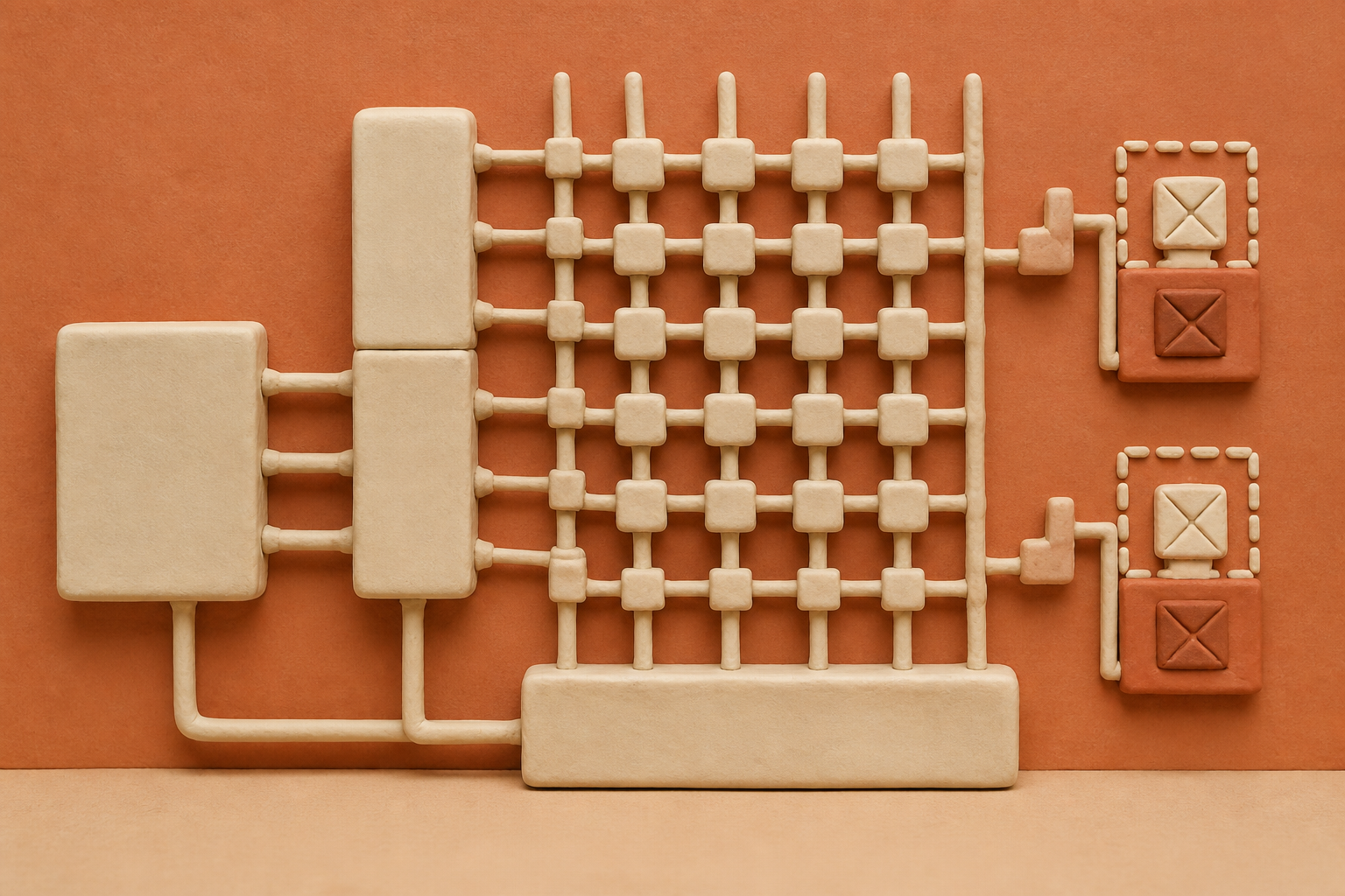
What changes in this design
With two places for programmed information, a reader might expect both to respond alike when programming is attempted.
Here, the result is uneven: one of the two rear-side places is programmed while the other fails to be programmed.
That mismatch is the main situation called out in the record. It shows that the two places can end a programming attempt in different conditions.
A $20,000 prize and four ways in
Raspberry Pi put $10,000 on a single row of memory. Row 0xc08 of the RP2350 chip held a secret in one-time-programmable storage, and anyone who could read it out could have the money. Nobody collected by the original deadline, so the prize was extended to the end of 2024 and doubled.
Four valid submissions arrived. All four teams were paid the full $20,000, and the attacks had almost nothing in common: one manipulated the power supply during a guard read, one glitched the USB bootloader with voltage, one fired a laser at the exposed die while it checked a secure-boot hash. The fourth just looked at the memory through a microscope.
One day of prep, a few hours of beam time
That fourth one is why the rest of this matters. A team at IOActive published it in January 2025, and they don't hedge: manufacturers and IP vendors "have claimed for years that antifuses are a high security memory which is significantly more difficult for an attacker to extract data from than other types of memory... however, as our results show, this is untrue."
An antifuse stores a bit by deliberately breaking down a thin gate dielectric: blown or not blown, once, permanently. That difference is visible. Using passive voltage contrast on a dual-beam microscope, the team pulled a full bitplane of 4,096 bits off a commodity 40nm microcontroller in about an hour, with over a hundred grey levels separating programmed cells from unprogrammed ones, clean enough for machine vision to read automatically. One day of sample prep, a few hours of beam time, a single chip. Beam time rents at roughly $200 an hour. The broken block wasn't obscure. It was licensed IP sold as protection "against active and passive attacks, tampering, hacking, and reverse engineering," shipped by its owner's count in more than 10 billion units.
Chaffing: store the complement in the neighbouring cell
The attack has one limitation, and the limitation became the fix. Adjacent rows share metal 1 contacts, so what the microscope actually reads is the bitwise OR of two physically neighbouring cells. Store {0, 1} or {1, 0} in every pair and the reader always sees all 1s. Raspberry Pi published exactly that, along with advice to keep secrets "as larger blocks of chaffed data, from which the secret is recovered by hashing." The researchers named the same countermeasure, then cautioned that refinements they were already developing might defeat it.
Five weeks later, a provisional application
Five weeks later, on 27 February 2025, TSMC filed a provisional. The full application followed in August 2025 and published this August as US20260253623A1, "Memory Circuit and Method of Forming the Same."
It describes a cell with two storage elements sitting on the back side of the substrate, each with its own selection transistor, and a word line transistor on the front. During programming one element is programmed and the other, in the filing's own words, fails to be programmed. Never both. The stated purpose is that reverse engineering of the circuit becomes more difficult, with enhanced security in physically unclonable function applications.
I can't show one caused the other, and the calendar doesn't prove it. But it's the same mechanism. What changed is where it lives: chaffing as published is a convention a designer follows, and conventions get skipped. Here the pairing is the cell itself.
The back side was supposed to carry power
Why the back side? Because that silicon is about to stop being inert. Researchers at imec measured buried power rails cutting IR drop about 1.7 times, and backside delivery through nano-scale through-silicon vias cutting it roughly seven times. TSMC's A16 node goes further, wiring power straight into transistor source and drain regions.
The tolerances say a lot about the difficulty. Rails around 30nm wide at 100nm pitch. Vias 320nm deep. Wafers thinned to a few hundred nanometres of silicon, thickness variation under 40nm, overlay alignment better than 10nm. That's the envelope a back-side cell lives inside. And the node is running late: reporting in April put A16 volume production in 2027, a year later than expected. TSMC's own page for it publishes no dates and no numbers.
Where this leaves things
What strikes me is the speed. A hack published for free, with its fix written into the same public writeup, turns up as foundry process architecture within a year. That's quick, and it happened in the open.
I'd hold the security claim loosely, though. The people who broke the old memory said their suggested mitigation might not survive the refinements they were already working on. A pairing built into the cell can't be forgotten by a designer. That's worth something. It isn't proof against the next microscope. And the barrier was never a state actor: a few hundred thousand dollars of equipment, a week or two learning the part, then a day or two per chip.
Sources
Reporting for this piece drew on the published filing and the references below.
- Memory Circuit and Method of Forming the Same - US Patent Application 20260253623
- Extraction of Secrets from 40nm CMOS Gate Dielectric Breakdown Antifuses by FIB Passive Voltage Contrast (arXiv)
- Security through transparency: RP2350 Hacking Challenge results are in (Raspberry Pi)
- Novel Invasive Attack on One-Time-Programmable Antifuse Memory (IOActive)
- How to power chips from the backside (imec)
- TSMC unveils latest roadmap: A16 volume production delayed to 2027 (TrendForce)
The record, briefly. US20260253623A1, “Memory Circuit And Method Of Forming The Same” A memory circuit includes first and second back-side storage elements, first and second selection transistors, and a front-side first word line transistor; during programming, one storage element is programmed while the other fails to be programmed.
More angles on this
- A Sideways Reading of Split StaircasesAnother reading from the same G11C classification family, static stores.
- CPC G11C: Static storesThe official classification family this record was filed into, published in the USPTO Cooperative Patent Classification scheme.
- CPC H10B: Electronic memory devicesThe official classification family this record was filed into, published in the USPTO Cooperative Patent Classification scheme.
- Liquid Cooling Heat Dissipation Device For Multi-Disk Drive System Marks a Pause Worth NoticingAnother reading from the neighbouring G11B classification family, information storage based on relative movement between record carrier and transducer.
- The Clip Needs Its ContextAnother reading from the wider H04N classification family, pictorial communication, e.g. television.
Read around this one:Public patent recordUSPTO published figure