Machines
A Small Committee Before Stress
One small circuit in Kioxia's new filing points to the costly reliability test standing between MRAM's promise and its wider use.

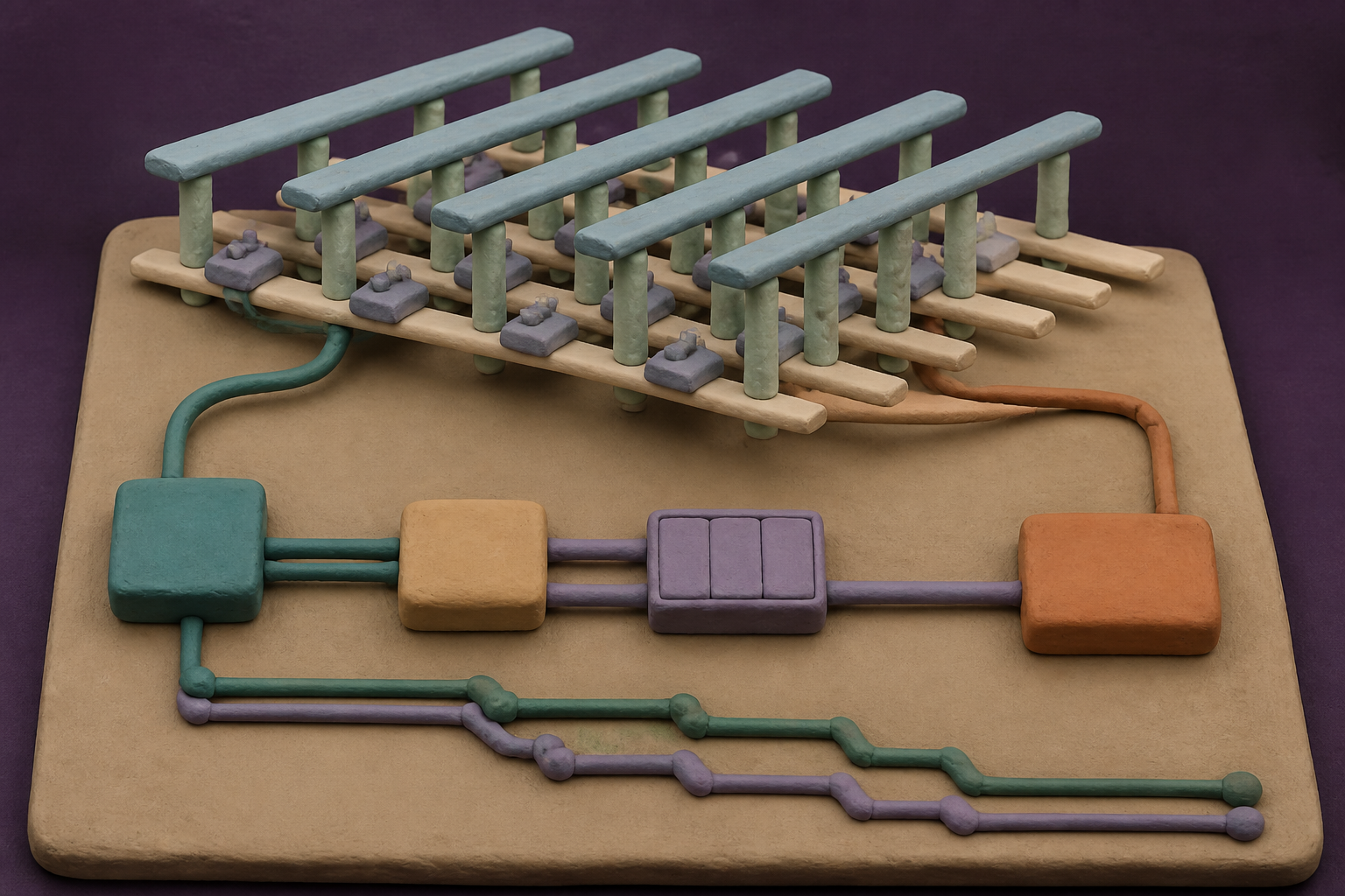
What changes in this design
A reader might otherwise assume that applying stress to a memory cell is a direct action, with the stress-producing part simply acting on the cell. This record makes clear that a decision comes before that action.
The first driver makes a potential from the cell terminal voltage. Comparing that potential with a reference produces data for a register. The register controls whether the second driver applies stress to the memory cell.
The key point is that stress is not presented as automatic. Its application depends on data from comparing an electrical level tied to the cell with a reference, while a register controls the result.
Forty-eight hours
Forty-eight hours is a long time to wait for a memory chip to reveal that it will fail early. The 48-hour burn-in used to screen a current high-reliability MRAM product is why I began there: the part is stressed in the factory so early-life failures appear before it reaches a system expected to keep working. Everspin advertises that process on its PERSYST xSPI parts, alongside temperature, radiation, and retention claims.
That number changes how I read a fresh patent filing. A test that lasts two days is not a footnote to a memory business. It is time, equipment, energy, and a decision about which cells are trusted. For MRAM, the problem is not merely making a bit switch. It is showing, cheaply and repeatedly, that the magnetic tunnel junction behind that bit will keep behaving after stress.
An August shareholding
The pressure around that problem is unusually large. In August 2026, reporting on Kioxia's ownership described SK hynix as the de facto shadow largest shareholder through convertible bonds held in the vehicle that was then the formal largest shareholder. Its voting rights are contractually capped at 15 percent until 2028, pending antitrust approvals. That is not a completed takeover. That distinction is one we should keep clear. But it does put a rival's long-term financial stake beside the company filing this patent.
A patent application isn't, to me, a window into boardroom motive. It is better evidence of a technical bet: even in a company associated with flash memory, the company is still spending attention on MRAM's hard, unglamorous reliability work. The application was filed June 17, 2025, claims a Japanese priority filing from February 25, and published August 27, 2026. Its timing overlaps the ownership story, but the filing does not explain why it was made.
A second driver
US20260253627A1 is titled Memory Device, a bland name for a pointed idea. A first driver turns the voltage at a memory-cell terminal into a potential. A comparison circuit checks that potential against a reference, and a register uses the resulting data to decide whether a second driver should apply stress when an external instruction calls for it. That reads to me as an attempt to bring a screening decision closer to the cell, rather than treating every cell as equally fit for the same punishment.
That last sentence is interpretation, not a proven production result. The filing describes a circuit arrangement and a control path; it does not establish that a commercial chip will cut test time, lower cost, or improve yield. Still, it directly addresses the point at which screening gets expensive: deciding how a particular cell responds before imposing more stress.
Sixty-four gigabits
The surrounding research makes the filing, I think, more consequential than its title suggests. Kioxia has also presented work toward a 64 Gbit MRAM, and its researchers have proposed a ring-shaped cell intended to improve stability and resistance to outside magnetic fields at high density. Those are two different fronts: make the cell denser and tougher, then find the weak ones without devoting that much factory time to every part.
But this doesn't, I think, mean MRAM is on the verge of displacing the familiar memory hierarchy. A January analysis from a memory specialist points to write-current, shared read-write path, density, and cost constraints. It calls SOT-MRAM promising for speed and endurance but not yet mass-producible. Better screening can remove one obstacle. It cannot settle all the others.
What would have to be true
For this particular circuit to matter beyond a patent file, several things would have to line up. The voltage-derived comparison would need to identify cells that really are prone to early failure, rather than rejecting healthy cells. The register and second driver would need to add less area, power, and design complexity than the test capacity they save. And the stress procedure would need to predict years of service without creating its own damage.
That is why I land on a modest but firm view. The interesting part is not that a chip can stress a memory cell. A current MRAM product is already put through two days of factory screening. It is that Kioxia is trying to make the decision selective and local. If the correlation is strong and the overhead is low, that could turn reliability screening from a long factory process into circuitry designed into the product. If not, MRAM remains a capable specialist memory with an expensive proof problem.
Sources
Reporting for this piece drew on the published filing and the references below.
- Memory Device patent - US20260253627
- SK Hynix-Funded SPC Becomes Largest Shareholder of Japan's Kioxia
- PERSYST xSPI MRAM: High-Reliability Memory for Mission Critical Applications
- Coherent Spin-Orbit Torque Magnetization Switching of Ring-shaped MTJ for High-density SOT-MRAM
- Kioxia's 64 Gbit MRAM at ISSCC 2025
- MRAM Can Replace SRAM/DRAM? - RAMXEED tech column
The record, briefly. US20260253627A1, “Memory Device” A first driver generates a potential from a memory cell terminal voltage. Comparison with a reference produces data that a register uses to control whether a second driver applies stress to the memory cell.
Identity details. The saved title-page transcription needs review, so names are not repeated here. Check the official published title page.
More angles on this
- A Sideways Reading of Split StaircasesAnother reading from the same G11C classification family, static stores.
- CPC G11C: Static storesThe official classification family this record was filed into, published in the USPTO Cooperative Patent Classification scheme.
- Liquid Cooling Heat Dissipation Device For Multi-Disk Drive System Marks a Pause Worth NoticingAnother reading from the neighbouring G11B classification family, information storage based on relative movement between record carrier and transducer.
- When a Vehicle Notices Something, Who Decides What the Moment Means?Another reading from the wider G06V classification family, image or video recognition or understanding.
- Editing at the Distance of a FrameAnother reading in the same Machines category on this site.
Read around this one:Public patent recordUSPTO published figure