Machines
The Doorbell Before the Parcel
An obscure memory-bus patent lands in the middle of an AI storage surge, a giant NAND acquisition, and a regulator's expiring price cap.

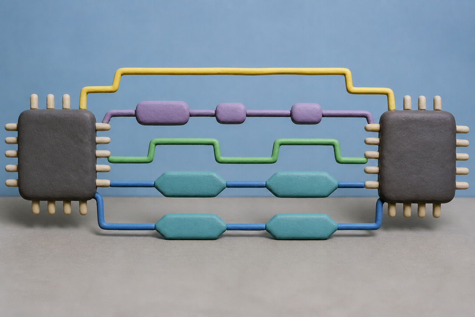
What changes in this design
Without this timing arrangement, a reader might simply expect the chips' control instructions and their data exchange to be treated as one continuous interaction.
This record says the first chip supplies chip-enable and command-address signals while the second performs an internal operation. After a selection chip-enable command, the second sends data to, or receives data from, the first memory device.
For a non-specialist, the key point is timing: selecting and directing the second chip comes before the later data transfer. That makes the system easier to picture as a handoff between two chip parts.
March 13's storage number
On March 13, 2026, a market report put the previous quarter's revenue for the five largest enterprise SSD makers above $9.9 billion. That was 51.7 percent higher than the quarter before. That report gives scale to a normally hidden part of computing, which is why I started there. SK hynix and Solidigm together accounted for $3.26 billion, up more than 75 percent in one quarter, and 30.2 percent of the market. A recent U.S. patent filing from SK hynix is not the cause of those figures. That filing is, I think, evidence of the interface work that this kind of storage growth makes valuable.
The 4,800 MT/s bus
JEDEC's November 2024 JESD230G standard added a separate command/address, or SCA, bus protocol to NAND flash interfaces. It specifies speeds up to 4,800 MT/s, versus 400 MT/s in the original 2011 standard. The difference reads to me as a change in the kind of bottleneck worth worrying about.
SCA doesn't strike me as a private language belonging to its filer. The protocol is an open, cross-industry standard, developed through cooperation among firms that had backed competing NAND interface camps. That matters to me. The patents in this story are not claiming an entire connector. They are arguing over how devices take turns after the connector exists.
April 2023, between closings
On April 7, 2023, SK hynix filed the application family that includes this publication while its $8.85 billion purchase of a rival's NAND business sat between two closings. The first phase had closed in December 2021; the final $1.9 billion payment came on March 27, 2025. That timing isn't proof, to me, that the acquisition caused this design. It does put the filing inside a period when the company's NAND operation was being substantially enlarged.
After the final closing, the buyer had acquired NAND intellectual property, research staff, and a manufacturing site in Dalian. SK hynix reported FY2025 revenue of 97.1467 trillion won and operating profit of 47.2063 trillion won. It also said NAND reached its highest annual revenue, helped by second-half enterprise SSD demand and QLC SSDs for AI data centers, while development of 321-layer QLC NAND was completed. None of that will, in my view, become proof that one scheduling idea made the difference. The evidence supports a narrower point: moving data among NAND devices had become commercially consequential.
A shared data bus
The filing, US20260253625A1, concerns two semiconductor apparatuses on a system. The first supplies chip-enable and command-address signals. The second does internal work, then, after a selection chip-enable command, either sends data to the first or receives it from the first memory device. The consequential detail is, I find, in the timing. The related granted patent describes selection, disable, and termination commands that can give each NAND die its own data-input/output period even when the dies share one data bus.
That is not a proposal to give every device a private data bus. It is, to me, a scheduling claim: preserve the shared bus, but set a distinct window for a chosen die. The related granted patent names the two pressures behind it. In the older shared-bus arrangement, command overhead worsened as frequency rose. SCA separated command and address traffic, but made parallel work across multiple NAND flash devices difficult. An independent I/O period is the attempt to make both facts less painful.
The harder half of the problem
The engineering win is, I think, not the harder story. The harder story is who can turn a shared standard into market power. In December 2021, China's competition regulator cleared SK hynix's acquisition subject to five years of conditions. One capped the company's Chinese-market PCIe and SATA enterprise SSD prices at their trailing 24-month average. The regulator calculated that the merger, without conditions, would push global SATA enterprise SSD share above 90 percent and global PCIe enterprise SSD share above 80 percent. The price cap is expected to expire around the end of 2026.
A filing from a rival Korean manufacturer uses the same SCA pin architecture differently. During a data transfer lasting 10 to 900 microseconds, it reads noise-state data over the command/address line, so monitoring does not consume data-bus bandwidth. That is, to me, the real shape of this contest. The standard is shared; the refinements are not. This SK hynix filing matters not because it foretells a gadget, but because it records a fight over small intervals on infrastructure serving an AI-storage surge. The scale is one we should keep straight: a clever timing patent is evidence of the contest, not its whole explanation.
Sources
Reporting for this piece drew on the published filing and the references below.
- US20260253625A1 - Semiconductor Apparatus And Semiconductor System Having Independent Data Input/Output Period
- US12424250B2 - Semiconductor apparatus and semiconductor system having independent data input/output period
- JEDEC specs JESD230G for improved NAND Flash interface speeds
- SK hynix finalizes acquisition of Intel's NAND business, takes full control of Solidigm
- Q4 2025 top-5 enterprise SSD revenue up over 50% QoQ
- SK hynix Announces FY25 Financial Results
- China's antitrust bureau conditionally approves SK Hynix's purchase of Intel's NAND memory chip business
- US20250166670A1 - Non-volatile memory device, storage device including the same
The record, briefly. US20260253625A1, “Semiconductor Apparatus And Semiconductor System Having Independent Data Input/Output Period, And Operating Method Of The Semiconductor System” A semiconductor system has first and second semiconductor apparatuses: the first supplies chip-enable and command-address signals, the second performs an internal operation, and after a selection chip-enable command the second transmits data to the first or receives data from the first memory device.
More angles on this
- A Sideways Reading of Split StaircasesAnother reading from the same G11C classification family, static stores.
- CPC G11C: Static storesThe official classification family this record was filed into, published in the USPTO Cooperative Patent Classification scheme.
- Liquid Cooling Heat Dissipation Device For Multi-Disk Drive System Marks a Pause Worth NoticingAnother reading from the neighbouring G11B classification family, information storage based on relative movement between record carrier and transducer.
- When a Vehicle Notices Something, Who Decides What the Moment Means?Another reading from the wider G06V classification family, image or video recognition or understanding.
- Editing at the Distance of a FrameAnother reading in the same Machines category on this site.
Read around this one:Public patent recordUSPTO published figure