Field Notes
Memory Array Marks a Pause Worth Noticing
A patent for a memory cell that stores nothing turns out to be the residue of a Chinese institute building its own RRAM line after the qualified route closed.

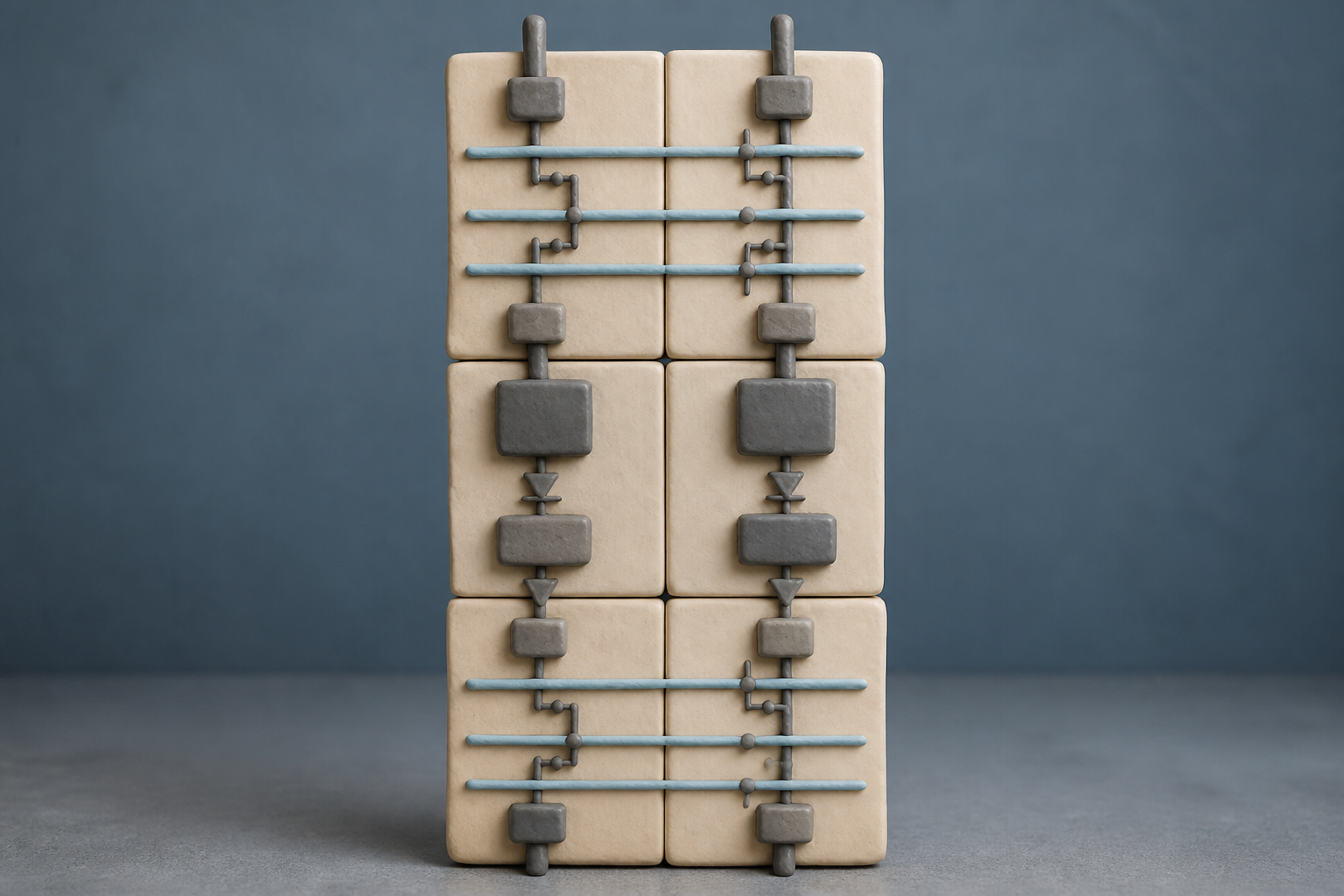
What changes in this design
Without further detail, a reader might picture a memory array as simply its primary collection of cells.
Here, at least one larger extra cell sits next to a main-array cell. It shares that cell's bit line, an electrical pathway, and needs less voltage in the forming step.
That is worth knowing because the setup is connected here to the main cell's high-resistance starting state and to improved yield, or how many arrays turn out usable.
A shuttle run opens in Jimei District
On March 22, 2024, an institute in Software Park Phase III, in the Jimei district of Xiamen, put on a technical exchange for engineers from four Chinese universities. The subject was a service, not a paper; I think that matters. Xiamen Industrial Technology Research Institute was opening its 28nm resistive RAM process to outside customers: its own recipe, certified by a foundry partner, now in commercial service.
The terms it publishes are the terms of a small business. Minimum tape-out area 3 square millimetres. Sixty bare dies back. Under four months from tape-out to wafer-out, roughly ten days for masks and a hundred and ten for manufacturing. Two shuttle runs a year. And a number in the specification sheet: operating bit yield above 99.9 percent.
Every cell needs one high-voltage jolt first
Resistive RAM stores a bit as a conductive filament grown through an oxide layer. Before any of that works, each fresh cell needs one high-voltage pulse to grow that filament for the first time. This is called forming, and it is not a Chinese quirk. One of the Western vendors, Weebit Nano, describes the same one-time positive voltage across the switching layer in its own bitcell, using standard fab materials at 130nm and scaling toward 22nm.
Nobody has abolished the step. It matters commercially, I think, because flash embedded on-chip stops scaling below 28nm, and cars now want two to thirty-two megabytes of it. Something has to replace it.
A larger cell that stores nothing
So: the filing. On June 8, 2023 the Xiamen institute filed in China; a PCT followed in June 2024, and the US publication landed on August 27, 2026 as application 18/994,087. Its title is Memory Array.
What it describes is a main array plus at least one dummy array - cells that store nothing. A dummy resistive cell shares a bit line with a neighbouring real cell and is deliberately made larger, so it forms at a lower voltage, which I find more revealing than the title. That lets the real cell start life in a high-resistance state. The stated purpose is improving the yield of the array. It is the same number the institute is selling.
What the 2015 hafnium-oxide numbers show
Does it work? The physics behind the assumption is public, and it is older than the patent, which I find telling. A 2015 in-line study of hafnium-oxide crossbars on 300mm wafers measured forming voltage falling as cells got bigger: 2.78 volts at 50 by 50 nanometres, 2.54 at 100, 2.18 at 200. That is the effect the filing leans on.
But the spread went the other way. Total standard deviation ran 0.17, 0.15, then 0.22 volts, so relative variability widened from about 6 percent to 10. A deliberately oversized reference cell is easier to form and noisier. The same paper formed 23 of 24 chips. The one that failed needed over 4 volts.
The footnote on Weebit's licensing slide
Here is why I think the workaround exists. Ten weeks before that Chinese priority date, a Taiwanese memory IP house and its foundry partner announced qualified 8-megabit RRAM on a 22nm low-power process. Buying qualified IP was a live option. Then it was not, for some buyers.
Weebit's own conference slide offers to license its technology to any fab, with a footnote: except US blacklisted. On December 2, 2024, the Bureau of Industry and Security added 140 entities to the Entity List, controlled 24 types of chipmaking equipment and three categories of development software, and pulled high-bandwidth memory under the foreign direct product rule. Tools and memory. Exactly what a domestic line runs on.
What would have to be true
For this dummy array to be more than housekeeping, the oversized cell's forming voltage would have to be predictable enough that its extra noise does not eat the margin it buys. The 2015 numbers say that is a real trade, not a free one, and the filing does not publish its own distributions. I would also want to know what happens at the second cycle and the thousandth, not just the first.
The institute's later results claim endurance in the tens of millions of cycles and sixteen resistance states, presented at a conference in late 2024 - a different claim, on a line that has since gone into service. Read alone, this patent is a small fix. Read in sequence, it is what building your own memory looks like when buying it stops being possible.
Sources
Reporting for this piece drew on the published filing and the references below.
- US 2026/0253620 A1, "Memory Array" (USPTO published application)
- Memory Array - US Patent Application 20260253620 (Justia)
- CMOS+RRAM Tape-Out Service - Xiamen Industrial Technology Research Institute
- Xiamen Institute holds RRAM external tape-out service technical exchange
- Xiamen Institute RRAM results presented at IEDM 2024
- eMemory and UMC Expand Low-Power Memory Solutions with 22nm RRAM Qualification
- In-Line-Test of Variability and Bit-Error-Rate of HfOx-Based Resistive Memory
- Weebit ReRAM in commercial fabs for AI edge applications (FMS 2025)
- Weebit ReRAM Bitcell - Technology
- Commerce Strengthens Export Controls to Restrict China's Capability to Produce Advanced Semiconductors
The record, briefly. US20260253620A1, “Memory Array” Describes a memory array with a main array and at least one dummy array. A dummy-array resistive cell shares a bit line with an adjacent main-array cell and is larger, with lower forming voltage, enabling the initial main-array cell state to be high resistance and improving yield.
More angles on this
- A Sideways Reading of Split StaircasesAnother reading from the same G11C classification family, static stores.
- CPC G11C: Static storesThe official classification family this record was filed into, published in the USPTO Cooperative Patent Classification scheme.
- CPC H10B: Electronic memory devicesThe official classification family this record was filed into, published in the USPTO Cooperative Patent Classification scheme.
- Liquid Cooling Heat Dissipation Device For Multi-Disk Drive System Marks a Pause Worth NoticingAnother reading from the neighbouring G11B classification family, information storage based on relative movement between record carrier and transducer.
- The Clip Needs Its ContextAnother reading from the wider H04N classification family, pictorial communication, e.g. television.
Read around this one:Public patent recordUSPTO published figure