Field Notes
The Tilted Rim: An Editor's Reading of an Asymmetrical SiC Substrate
A fresh patent on an old wafer size appears just as silicon-carbide manufacturing turns toward larger discs.

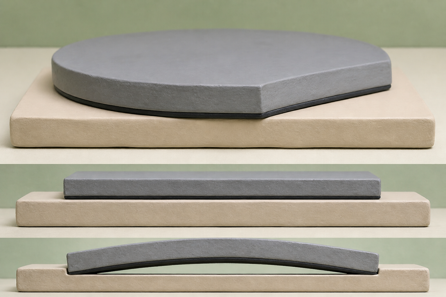
What changes in this design
Without the rim detail, a reader might picture a substrate with a main area and a regular outer edge. The record gives no broader comparison with other cutting methods.
Here, the outer region next to the main area is asymmetrical and slopes inward. The rim is made by moving multiple cutting wires in a nonlinear way.
The detail matters because heat-related deformation is the problem named here. The inward slope is meant to make the substrate more resistant to that change in form.
A wafer at 1,500 degrees C
At more than 1,500 degrees C, a silicon-carbide wafer can lift from its support plate during the high-heat step that lays down a crystal layer. A gap opens. Uneven temperatures bend the disc, opening a gap beneath it; carrier gas can then reach the exposed back side and leave deposits where they do not belong.
That gap, for me, turns a flatness problem into a manufacturing-loss problem. Damage follows. The wafer can bow or warp, while total-thickness variation makes later processing less predictable and cuts yield. This is physical: a hot disc no longer sits flush.
A rim cut on a curve
US20260255640A1 brings me to an earlier, identically titled application: Monocrystalline SiC Substrates Having an Asymmetrical Geometry and Method of Producing Same. Here, the answer isn't a new coating. No new furnace. The structural change I found at the wafer's edge is a main region beside an adjoining peripheral region that slopes inward. Its stated purpose is greater stiffness against heat-driven deformation.
Manufacturing detail makes the proposal concrete. A multi-wire saw cuts the asymmetric shape by moving a wire web along a nonlinear path, rather than a straight one. The earlier application describes an inclined peripheral region 15 to 60 micrometres tall, with 25 micrometres preferred. This is, in my simple reading, an attempt to preserve shape when heat is most punishing.
The uncertain family link
Care is necessary about whose attempt this is. An earlier, identically titled US publication names SiCrystal GmbH in Nuremberg and lists Kuniyoshi Okamoto and Michael Vogel as inventors. Its priority date is April 14, 2021. Filing followed in 2022. Publication came in October 2023; a grant followed on May 12, 2026.
Whether US20260255640A1 itself names SiCrystal is something I can't directly confirm. Direct lookup failed: the public page was inaccessible, and the exact number had not appeared in the patent database used there. That limit matters. Taken together, the title and family match make SiCrystal likely, not certain. So I won't treat the company connection as settled.
A $230 million six-inch deal
Here, timing is compelling. SiCrystal and STMicroelectronics expanded their 150mm SiC wafer supply agreement in April 2024, with a minimum expected value of $230 million. Behind it was a 2020 agreement reported at more than $120 million. Neither contract proves that this rim design was bought or deployed. Instead, they show that six-inch wafers still mattered commercially.
At that scale, a few micrometres at the edge can matter. For a manufacturer with a 150mm process, protecting output depends on preserving yield and flatness. It's practical. A supply agreement should not be mistaken for a forecast, but we should not write off the format prematurely.
The eight-inch pivot
But the wider market is hard to ignore. By Q4 2024, six-inch SiC substrate prices in China had reportedly fallen to about $400 or less, at or below cost. That drop was sharp. Eight-inch prices fell from roughly $3,000 to $4,000 at the end of 2023 to about $1,500 by mid to late 2024. By late 2025, one market analysis called this a necessary correction phase, with upstream boule and wafer utilization around 50 percent.
March 2026 brought Wolfspeed's completed 150mm Durham shutdown and a full shift to 200mm at Mohawk Valley. Elsewhere, other producers were ramping eight-inch capacity, including a China joint venture targeting about 480,000 wafers a year. On July 1, 2025, Wolfspeed filed for Chapter 11 and emerged after restructuring on September 30, 2025. That bankruptcy isn't a single-format verdict, to me. Prices collapsed while capacity outran demand, and the shift in diameter added another pressure. No single cause is proved.
What the filing is really betting on
The filing, in my view, is betting on industrial change's long tail. Older 150mm lines do not stop producing costly defects just because 200mm is the preferred destination for new capacity. They still run. If a shaped edge reduces heat-induced deformation, the payoff is more stable wafers and possibly better yield in plants that still run the older diameter. Yet no factory result is proved by the filing.
Nor is this the only route to flatter SiC. There are alternatives. Wolfspeed holds a separate 200 to 205mm wafer patent that addresses bow through a changing radial doping profile, rather than a machined edge. More than 320 substrate and epitaxial-wafer publications appeared in the first quarter of 2026, covering nearly 250 inventions. US20260255640A1 is, to my eye, a claim on a narrow, valuable problem - not evidence that the move beyond six inches has reversed.
Sources
Reporting for this piece drew on the published filing and the references below.
- US20230317780A1 - Monocrystalline SiC Substrates Having an Asymmetrical Geometry and Method of Producing Same
- SiCrystal GmbH - Your European Supplier for Silicon Carbide Wafers
- ROHM Group Company SiCrystal and STMicroelectronics Expand Silicon Carbide Wafer Supply Agreement
- Oversupply of 6-Inch SiC Substrate Leading to Price Decline
- Power SiC Faces Overcapacity Downturn Until 2027-2028, Before Device Market Grows to Nearly $10bn by 2030
- Wolfspeed Completes Financial Restructuring, Emerges From Chapter 11
- Wolfspeed Gets Grant for Silicon Carbide Wafers With Reduced Deformation and Bowing
- SiC Patent Activity Remains Dynamic
- Wafer Capacity Set to Surge: A New Phase for the SiC Industry in 2026
The record, briefly. US20260255640A1, “MONOCRYSTALLINE SiC SUBSTRATES HAVING AN ASYMMETRICAL GEOMETRY AND METHOD OF PRODUCING SAME” A monocrystalline SiC substrate has a main region and a peripheral adjacent asymmetric region inclined inward to enhance stiffness against thermal induced deformations; a multi-wire sawing process forms the asymmetric shape through nonlinear wire-web travel.
Identity details. The saved title-page transcription needs review, so names are not repeated here. Check the official published title page.
More angles on this
- A Memory Device That Treats the Edge as a Place to ThinkAnother reading from the same H10D classification family, inorganic electric semiconductor devices.
- CPC H10D: Inorganic electric semiconductor devicesThe official classification family this record was filed into, published in the USPTO Cooperative Patent Classification scheme.
- CPC B28D: Working stone or stone-like materialsThe official classification family this record was filed into, published in the USPTO Cooperative Patent Classification scheme.
- The Substrate That Gave Its Two Recesses Unequal DepthAnother reading from the neighbouring H10F classification family, inorganic semiconductor devices sensitive to infrared radiation.
- The Reply Arrow's Quiet HandoffAnother reading from the wider H04L classification family, transmission of digital information, e.g. telegraphic communication.
Read around this one:Public patent recordUSPTO published figure