Objects
When a Stack Needs a Voice at Start-Up
Behind the big HBM4 numbers, one new filing reveals the boot-up wiring that can decide whether a stacked memory chip works at all.

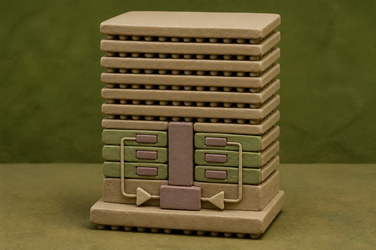
What changes in this design
Without the details here, a reader might picture stored start-up information leaving its storage circuit and traveling through the chip as a single path.
Instead, the device has multiple chip layers over a base layer. Each chip layer has two channel regions, each with a repeater - a small signal booster - that receives and strengthens fuse data at boot-up.
This identifies where start-up handling occurs across the stacked chip. It does not state what the data means or what follows after its signal is strengthened.
June's third failure
In June 2025, a major memory supplier failed a customer's HBM3E qualification for the third time. Reports tied the problem to heat and power. A component can promise huge bandwidth, then lose its place in a system over the work of moving heat, power, and signals through a stack, which is why I began there.
That customer was Nvidia, and SK hynix was its primary supplier of high-bandwidth memory, or HBM. A 2026 forecast estimated SK hynix supplied 91 percent of Nvidia's HBM in 2023 but projected 54 percent in 2026 as two rivals gained ground. It is only a forecast, but I take the direction seriously: the race has moved from who can stack memory first to who can make every layer start, talk, and keep working together.
The 2,048-bit interface
That pressure is visible in the HBM4 standard, published in April 2025. It specifies a 2,048-bit interface, 32 channels, and up to about 2 TB/s per stack. More routes and dies mean less room for an error to hide. The standard allows stacks of four, eight, 12, or 16 dies, with capacities up to 64 GB.
The history deserved a backward look, I thought. SK hynix says it built the industry's first HBM in 2013 by stacking DRAM dies with through-silicon vias, taking data paths from eight on a conventional DRAM chip to 1,024. It began HBM3 mass production in 2022. That history doesn't read to me as a secure lead. It reads to me as evidence that the hard work has always been inside the stack.
Boot-up fuse data
That brings me to US 2026/0253630, Memory Devices For Forming Data Paths. The filing names SK hynix as assignee, claims priority from a Korean filing on February 25, 2025, was filed in the United States on June 17, and published on August 27, 2026. Its earliest date came weeks before HBM4's April release. That is interesting, but it cannot tell us why it was filed.
This is not a filing for a higher headline bandwidth number. It describes core dies stacked on a base die. Each core die has two channel regions, each with a repeater that receives and amplifies fuse data during boot-up. The same repeaters handle repair data sent from the base die through a transmission circuit. The unglamorous constraint I see at the center of a remarkable package is this: boot-time fuse and repair information has to arrive strongly enough, in the right place, before the memory can do anything else.
Repeaters on the route
The patent's use of repeaters did not appear from nowhere. In a 2019 published application, SK hynix placed repeater blocks between memory-bank regions and I/O transmission lines to re-drive read and write data over longer on-die routes. The newer document carries that general approach into fuse and repair data across stacked dies. The two filings don't reveal to me how much circuitry they share. The continuity I can see is simpler: long internal paths need a signal refreshed along the way.
The base die is changing, too. Reports on HBM4 describe customized base-die designs that are co-designed and made by a foundry. A direct link between that arrangement and this patent eludes me. But it makes the division of labor here more consequential: the base die sends repair data, while the core dies re-amplify it. That handoff becomes harder to ignore, I think, when different specialists shape different parts of the stack.
Where this leaves things
By early 2026, a rival had begun volume shipments of a 12-high HBM4 product for Nvidia, reporting pin speeds above 11 Gb/s and bandwidth above 2.8 TB/s. Those figures do not make this application obsolete. They clarify why I find it revealing. A standard can add channels and a product can set a faster speed, but each stack still has to wake up with its own fuse and repair data intact.
This is not what I'd call a patent for the future of memory. It is narrower, and more useful than that. It records where the contest can be decided once the glamorous numbers are already on the slide: on a path from a base die to the layers above it, at boot, in a signal that must survive the trip. That is why I think it deserves attention. The filing reads to me as evidence that a small, necessary part of the stack is worth claiming just as customers and competitors have more choices.
Sources
Reporting for this piece drew on the published filing and the references below.
- Samsung predicts profit slump as its HBM3e underwhelms
- JP Morgan: SK hynix is not forever No. 1 - the three HBM makers collide
- Become a Semiconductor Expert with SK hynix - HBM
- Memory Devices For Forming Data Paths - US 2026/0253630
- Data Control Circuit, and Semiconductor Memory Apparatus... - US 2019/0079672
- Next-gen Nvidia Rubin prototypes begin testing with leap to chiplet design and HBM4 memory
- Micron Begins Volume Production of HBM4 for NVIDIA Vera Rubin
The record, briefly. US20260253630A1, “Memory Devices For Forming Data Paths” A memory device has multiple core dies stacked over a base die. Each core die includes first and second channel regions with respective repeaters that receive and amplify fuse data stored in a fuse data storage circuit during boot-up.
More angles on this
- A Sideways Reading of Split StaircasesAnother reading from the same G11C classification family, static stores.
- CPC G11C: Static storesThe official classification family this record was filed into, published in the USPTO Cooperative Patent Classification scheme.
- CPC H10B: Electronic memory devicesThe official classification family this record was filed into, published in the USPTO Cooperative Patent Classification scheme.
- Liquid Cooling Heat Dissipation Device For Multi-Disk Drive System Marks a Pause Worth NoticingAnother reading from the neighbouring G11B classification family, information storage based on relative movement between record carrier and transducer.
- The Clip Needs Its ContextAnother reading from the wider H04N classification family, pictorial communication, e.g. television.
Read around this one:Public patent recordUSPTO published figure