Field Notes
A Slanted Beam in the Routine of Making Superconducting Wire
A quiet process patent from Sumitomo Electric lands where fusion's appetite for superconducting tape already exceeds the room to make it.

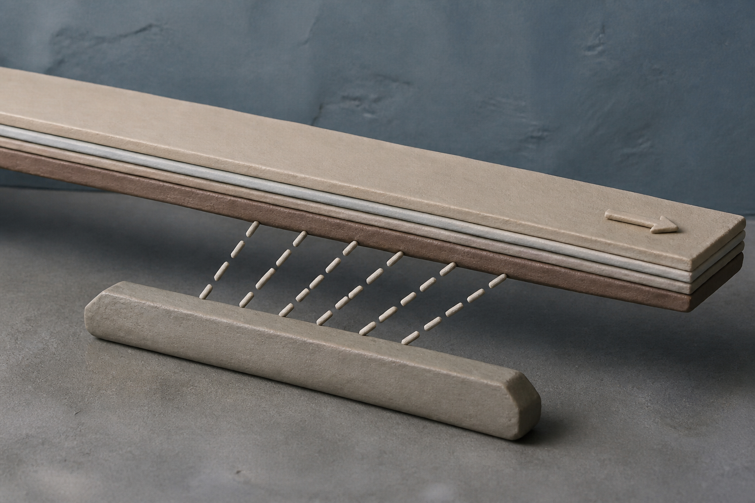
What changes in this design
Without more detail, someone might picture a surface being coated while it stays still, with material and a beam coming straight down.
Here, the base surface moves lengthwise while evaporated material is supplied and an ion beam approaches at an angle to the surface normal. The aim is to form the IBAD buffer layer during that movement.
This makes the method easier to understand: the surface moves while coating material is supplied and the ion beam is angled. No performance outcome or comparison is given.
186 miles of wire
In 2019 and 2020, Commonwealth Fusion Systems bought more than 186 miles of REBCO wire, in 400-to-600-metre lengths. That order was larger than some suppliers had made in the six years before it, a startling measure of how small this trade remained just before private fusion money arrived. The comparison matters because it turns an abstract supply-chain concern into a record of what manufacturers had actually been asked to deliver: one buyer's order could eclipse years of earlier output.
The squeeze is now easier to picture in tape, not venture slides. A prototype fusion reactor may consume about 10,000 kilometres of 4 mm REBCO tape, roughly 40,000 square metres of deposited film, while industry sources put global capacity in the same rough range. When I put those figures beside each other, the headline is not a miraculous magnet. It is a factory schedule with almost no slack. A single large project can therefore make capacity look ample in presentations and scarce in production planning at the same time.
A wide moving strip
Sumitomo Electric filed US 2026/0260788 A1 in May 2024, and it published on September 3, 2026. The application is not a new magnet design or a promise to make tape by the thousand kilometres. It concerns an early manufacturing step: laying an IBAD buffer layer on a moving substrate as evaporated material arrives and an ion beam strikes at an angle. That places the filing before the finished tape, at the stage where the material is being prepared to receive the layers that follow.
The details are unusually practical. Claim 1 calls for a substrate at least 15 mm wide and places the ion-beam source's long axis along that width, intended to improve texture uniformity. Other claims name magnesium oxide, Hastelloy or stainless-steel substrates, and a stack of underlayer, IBAD layer, and surface layer. The emphasis is on keeping a process controlled as the strip gets wider, rather than treating width as a simple increase in material. What I cannot tell from the published application is whether this tooling has entered production. A patent describes a protected method, not confirmed factory output.
Three ways to make texture
The choice of IBAD was never inevitable. Researchers at a Japanese wire maker proposed it in 1992, and a US national laboratory later refined it. RABiTS emerged at another US laboratory in 1996; inclined-substrate deposition followed in 1999 and reached commercial use in Germany. IBAD remains one of three competing ways to give a superconducting tape the ordered foundation it needs. The timeline also makes clear that the underlying manufacturing question is older than the recent fusion investment cycle.
Sumitomo Electric has reason to know this territory. It developed long-length oxide high-temperature-superconducting wire technology in 1996 and supplied cable that began carrying power on a US grid in 2006. For me, that history makes this narrow filing more interesting than a newcomer’s claim would be: it shows an old participant still working on the unglamorous constraint beneath the current rush. The filing does not need to announce a new market to show that process work remains active.
The price of film
Width helps only if the film remains usable from edge to edge. Leading makers together exceed 5,000 kilometres of annual capacity at 12 mm width, yet tape sells for roughly $15 to $30 a metre. Industry researchers describe short-term cost goals of $50 per kA-m and longer-term goals of $10 to $20 per kA-m, measures that price current-carrying performance rather than length alone. That distinction matters: more tape is not necessarily cheaper tape if the additional width does not deliver useful superconducting performance.
The filing makes no claim about cost or throughput. But I find its insistence on uniform texture across a wider strip revealing. Researchers identify below-50-percent material utilization in REBCO sputtering targets as a major cost driver, so manufacturing improvements have to protect both quality and waste. A wider substrate is not automatically more useful tape. The commercial test is not merely whether the strip can be made wider, but whether the process preserves the qualities for which customers are paying.
The harder half of the problem
Private fusion investment had reached about $9.77 billion by mid-2025, intensifying attention on the narrow supply of suitable conductor. One industry accounting of fusion-era REBCO suppliers does not include Sumitomo Electric in its roster. That omission proves little: I cannot establish from a supplier list whether this application signals a commercial return, a defensive patent position, or simply continuing process research. It does, however, keep the filing in the category of evidence about manufacturing work, rather than evidence of a confirmed production expansion.
The harder half is demand. An industry analysis warns that fusion timelines have “slipped repeatedly” and that no company has delivered grid electricity yet. I do not read that as a reason to dismiss better wire manufacturing. It is the reason to judge this patent at the proper scale: a credible attempt to improve one bottleneck, in a market whose biggest promised customer has not yet proved it can arrive. The tension is not between a real process constraint and an imaginary one, but between present manufacturing limits and a future demand case that remains unproven.
Sources
Reporting for this piece drew on the published filing and the references below.
- Commercial compact fusion triggered REBCO tape industry: PLD technology opportunities and challenges
- Commonwealth Fusion Systems
- Superconducting tapes: One big LEAP for fusion
- Advances in second-generation high-temperature superconducting tapes and their applications in high-field magnets
- Sumitomo Electric Industries
- REBCO Superconductors: Fusion Power's Rare-Earth Key
The record, briefly. US20260260788A1, “Method For Manufacturing Superconducting Wire” A superconducting wire is manufactured by forming an IBAD buffer layer on a substrate main surface while supplying evaporated constituent material and applying an ion beam inclined from the surface normal as the substrate moves longitudinally.
More angles on this
- Holding the Mechanical Line on a Hair-Thin WireAnother reading from the same H01B classification family, cables; conductors; insulators; selection of materials for their conductive, insulating or dielectric properties.
- A metal-MXene sandwich, and the quiet work of putting layers in the right orderAnother reading from the same C23C classification family, coating metallic material.
- CPC H01B: Cables; conductors; insulators; selection of materials for their conductive, insulating or dielectric propertiesThe official classification family this record was filed into, published in the USPTO Cooperative Patent Classification scheme.
- CPC C23C: Coating metallic materialThe official classification family this record was filed into, published in the USPTO Cooperative Patent Classification scheme.
- Inside electric vehicle adapter inspection deviceAnother reading from the neighbouring H01R classification family, electrically-conductive connections.
Read around this one:Public patent recordUSPTO published figure