Objects
At the Switch, Selective Erase Becomes a Question of Responsibility
One tiny adjustment to an erase pulse points to a larger fight over dense memory, chip identity, and the limits of stacked NAND.

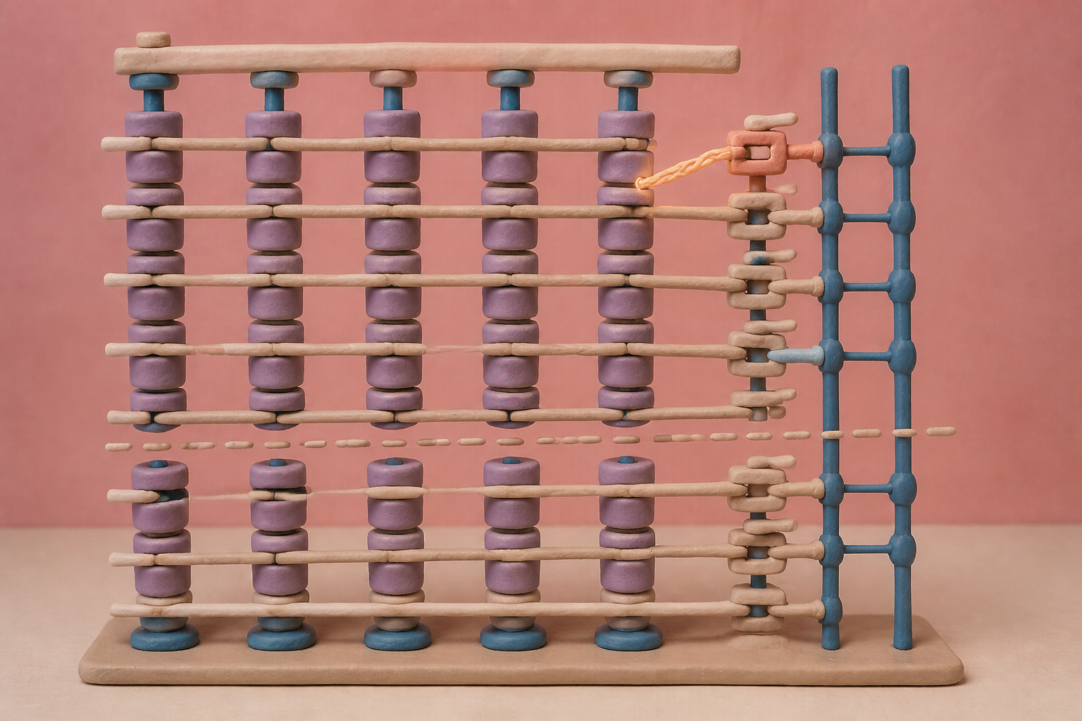
What changes in this design
A reader might assume that erasing memory simply means clearing cells, without needing to think about the switches and lines around them.
Instead, the first erase operation uses a control circuit to produce GIDL current at one drain selection switch and apply a lower voltage to another drain selection line.
That detail helps locate the action: selective erasing is associated with both a switch and a separate selection line.
321 layers, one stubborn operation
On August 25, 2025, SK hynix began mass production of a 2-terabit, 321-layer QLC NAND chip. The announced figures are unusually concrete: 56 percent faster writes, 18 percent faster reads, and 23 percent better write-power efficiency than its prior generation. What caught my attention was not the headline layer count but the operation that becomes harder as those layers pile up: getting old data out without needlessly tiring the rest of the chip.
That pressure sits underneath US20260253642A1, a U.S. publication titled Nand Flash Memory Device Capable Of Selectively Erasing Flash Memory Cell. It places word-line-connected cells behind drain-selection switches, which sit between the cells and bit lines. During a first erase operation, the control circuit generates GIDL current at a first switch while lowering the voltage on a separate drain-selection line. The filing gives us a specific electrical arrangement, not a demonstration that every individual cell in a production chip can be erased on demand.
Block erase
An earlier U.S. patent, US12444469B2, issued on October 14, 2025 with a near-identical title and the same GIDL approach. It looks closely related to this publication, though I cannot confirm the formal family link from the materials I reviewed. Its background describes the awkward status quo: NAND can write a single cell but generally erases a block. The extra program/erase work can degrade cells, especially in multi-level storage and in uses such as neural-network weights.
Selective erase is therefore not a cosmetic improvement. It would let the scale of removal track the scale of writing more closely, at least in principle. I don't read the new application as proof that it has solved endurance or made block erase obsolete. Its significance is more bounded: it proposes controlling one switch's GIDL current and another line's voltage so a chosen cell can be handled differently from its neighbours.
Three volts of GIDL
That same physical unevenness has already been made useful. A Seoul National University team and SK hynix used deliberately weak GIDL erase on commercial V-NAND to amplify cell-to-cell variation, then made that variation the basis of a physical unclonable function, a hardware-derived security key. A June 2025 account of the work reports 100 percent accuracy from 25 to 85 degrees C, validation over 10 million read cycles, and more than 100 conceal/reveal cycles.
Another paper from the collaborators tested a related physical unclonable neural network on commercial SK hynix TLC V-NAND with more than 100 layers. It used a 3 V weak erase against a stated 6 V standard erase. Cross-chip accuracy fell to about 20 percent, while a uniqueness measure reached 48.7 percent and the fingerprint remained stable through 10,000 conceal/reveal cycles. That reversal matters to me: a variation engineers normally try to control becomes the feature that distinguishes one chip from another.
Cold silicon, taller stacks
Variability, though, is not a free resource. A 2023 study calls GIDL erase a critical enabler for 3D NAND and identifies a hard scaling problem: higher stacks need more holes to raise channel potential. Its authors call that requirement a fundamental limitation on layer count as the industry pushes toward more than 1,000 layers.
The temperature result is blunter. Researchers found that GIDL current weakens when temperature falls, making cells harder to erase in both charge-trap and floating-gate designs. No source I read shows that US20260253642A1 removes that cold-condition constraint. Its fine-grained voltage control may help, but it still depends on a current whose strength changes with physical conditions.
The part worth watching
That is why the finance news belongs in this small electrical story. In July 2026, SK hynix raised $26.5 billion in a U.S. ADR listing. Reported plans for the proceeds included a Korean fabrication plant, a packaging plant, and EUV scanners for AI-driven memory demand. The company had already traced its stacking climb from 512Mb NAND in 2004 to 72-layer 3D NAND in 2017, 96-layer 4D NAND in 2018, and 321-layer 4D NAND by 2025.
The part worth watching is not a promise that every NAND cell will soon be independently erasable in ordinary use. For me, the filing matters because it records a design choice where density, endurance, temperature, and manufacturing variation meet. We should judge it by a plain test: whether selective erase reduces unwanted cycling in dense devices, and whether its GIDL tuning holds as stacks get taller and conditions get colder.
Sources
Reporting for this piece drew on the published filing and the references below.
- Nand Flash Memory Device Capable Of Selectively Erasing Flash Memory Cell
- NAND flash memory device capable of selectively erasing one flash memory cell and operation method thereof
- Self-Adaption of the GIDL Erase Promotes Stacking More Layers in 3D NAND Flash
- Seoul National University College of Engineering Research Team Develops Concealable PUF Using V-NAND Flash Memory
- Model-Inversion-Resistant Physical Unclonable Neural Network Using Vertical NAND Flash Memory
- Origin of the Temperature Dependence of Gate-Induced Drain Leakage-Assisted Erase in Three-Dimensional NAND Flash Memories
- [One-Team Spirit] The Miracle of 321 Layers
- SK hynix launches mass production of world's first 321-layer QLC NAND flash
- SK Hynix raises $26.5B in the biggest foreign IPO in US history
The record, briefly. US20260253642A1, “Nand Flash Memory Device Capable Of Selectively Erasing Flash Memory Cell” A NAND memory device has word-line-connected cells and drain selection switches between the cells and bit lines. During a first erase operation, a control circuit generates GIDL current at a first drain selection switch and applies a lower voltage to another first drain selection line.
Identity details. The saved title-page transcription needs review, so names are not repeated here. Check the official published title page.
More angles on this
- Non-Volatile Memory With Distributed Write: the erase step that sets the priceAnother reading from the same G11C classification family, static stores.
- A storage medium with two bosses, and the address that has to survive the handoffAnother reading from the same G11C classification family, static stores.
- CPC G11C: Static storesThe official classification family this record was filed into, published in the USPTO Cooperative Patent Classification scheme.
- The Substrate That Gave Its Two Recesses Unequal DepthAnother reading of a record filed by the same applicant, SK hynix Inc..
- The Light Loop Inside an Oral-Care RoutineAnother reading from the wider G06T classification family, image data processing or generation, in general.
Read around this one:Public patent recordUSPTO published figure