Field Notes
Memory Built in Layers, With a Staircase Cut Into the Edge
A new Micron memory filing shows why an old staircase still matters as an export-restricted rival enters the same high-layer contest.

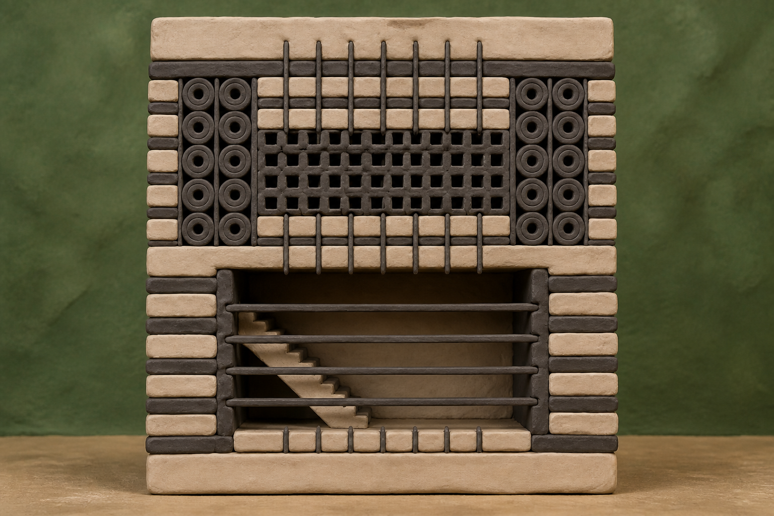
What changes in this design
Someone new to electronics may picture electrical paths spread across a flat surface rather than a structure built upward in layers.
Instead, it sets out a vertical stack of layers that either resist electricity or carry it. Strands pass through the stack, and a cavity in the stair-step section contains treads that carry electricity between two outer walls.
This makes the physical layout easier to picture: a stack, strands through it, and a cavity holding a staircase at one edge. No performance result or reason for choosing this layout is stated.
The 24-layer beginning
August 2013 is a useful place to begin. A 24-layer, 128Gb 3D NAND device reached the market after planar NAND scaling had run into trouble below about 20nm. Stacking memory vertically offered a way forward, but it also made access harder: a tier buried in the stack still needed a precisely placed electrical contact at its edge.
Early reporting identified staircase etching as a stubborn part of that job, with precise contact landing and resist pull-back already on the checklist. Other memory makers followed the next year. The staircase has endured as each additional tier adds capacity while making the route to individual conductive layers more demanding. It was a manufacturing constraint from the start.
The hidden staircase
The staircase is not the storage array itself. It is the stepped edge that exposes successively deeper conductive tiers so contacts can meet them. That distinction matters because a taller stack is not merely a taller version of the old device: the access geometry has to remain manufacturable at every depth.
A comparison of recent 3D NAND products puts a 232-layer Micron die at 14.60 Gb/mm2. The highest cited 232-layer example reached 15.03 Gb/mm2, while another 238-layer example came in at about 14.75. Those are measurements of particular products, not a universal league table, but their closeness makes small process improvements hard to dismiss.
Nor is a better staircase the only way to shrink a die. The same comparison points to cell-over-periphery designs and wafer-bonding approaches as rival paths. This filing is therefore less a claim to own the future of 3D NAND than evidence of a continuing contest over where the hardest manufacturing work belongs.
A cavity full of treads
US20260253638A1 belongs in this old, practical problem. Its title, "Memory Circuitry And Method Used In Forming Memory Circuitry," gives little away. Inside are alternating insulating and conductive tiers crossed by vertical strings of channel material. At the stair-step region, the filing describes a cavity containing a flight of stairs, with conductive treads spanning between laterally opposing outermost sidewalls.
The literal details are technical. I couldn't tell from the filing whether this exact arrangement has reached production, and it does not establish a yield gain or a lower-cost chip. The narrower point is that it records another effort to control the part of 3D NAND where contacts must find the correct depth. An earlier granted member of its Micron Technology patent family, filed August 29, 2022 and granted July 22, 2025, names John D. Hopkins and Alyssa N. Scarbrough and describes anisotropically etched spacers used as masks to form treads at varying depths. Related continuations make this look like ongoing work, not an isolated sketch.
128 layers and 14 percent
On October 7, 2022, the U.S. Commerce Department treated NAND with 128 layers or more as controlled advanced technology. YMTC was added to the Entity List that December. One account puts its spending on requalifying domestic equipment at roughly RMB96 billion from 2023 through March 2026.
By the second quarter of 2026, YMTC held 14% of global NAND shipments and ranked third. Its Xtacking 4.0 reached 267 layers, compared with 276 for Micron and 286 for two other leading producers. Shipment share cannot demonstrate technological independence, profit, or unrestricted access to equipment. Yet the narrower policy premise is difficult to sustain: the 128-layer boundary did not keep YMTC from competing far above it.
Xtacking's wafer-bonding architecture puts staircase refinement alongside another route to shrinking a die. The policy story and the patent story meet there: one company is refining the stairs, while another has helped make clear that stairs are not the only place to seek an advantage.
The open question
The question is not whether a staircase matters. It plainly still does. What I cannot infer from this filing is whether cavity-bounded treads, spacer masks, and finer steps will be the decisive route to denser memory, or whether designs that relocate more of the problem will matter more. The filing gives geometry, not an answer.
Micron reported $41.456 billion in third-quarter fiscal 2026 revenue, 84.6% GAAP gross margin, and $7.1 billion in net capital expenditures. Those facts do not explain this particular filing or prove it will reach production. They place it within a period of enormous investment in memory manufacturing. I think its modesty is the lesson: layer counts make headlines, but a contest this close is also decided at the edge of the stack, where every tier must still be reached.
Sources
Reporting for this piece drew on the published filing and the references below.
- Memory Circuitry And Method Used In Forming Memory Circuitry - US20260253638A1
- US12369321B2 - Memory circuitry and method used in forming memory circuitry
- 3D NAND: To 10nm and beyond
- Comparison: Latest 3D NAND Products from YMTC, Samsung, SK hynix and Micron
- Micron Technology Reports Results for the Third Quarter of Fiscal 2026
- The No. 3 NAND Maker Washington Couldn't Stop
The record, briefly. US20260253638A1, “Memory Circuitry And Method Used In Forming Memory Circuitry” Memory circuitry has vertically alternating insulative and conductive tiers, with channel-material strings extending through the insulative tiers and conductive tiers in a memory-array region. Its stair-step region has a cavity containing a flight of stairs with conductive treads extending between laterally opposing outermost sidewalls.
More angles on this
- Shift Register Unit, Driving Method Thereof, Display Substrate And Display Marks a Pause Worth NoticingAnother reading from the same G11C classification family, static stores.
- In-Memory Computation System Using A Segmented Memory Architecture With Marks a Pause Worth NoticingAnother reading from the same G11C classification family, static stores.
- CPC G11C: Static storesThe official classification family this record was filed into, published in the USPTO Cooperative Patent Classification scheme.
- CPC H10B: Electronic memory devicesThe official classification family this record was filed into, published in the USPTO Cooperative Patent Classification scheme.
- A metal-MXene sandwich, and the quiet work of putting layers in the right orderAnother reading from the neighbouring H10W classification family, generic packages, interconnections, connectors or other constructional details of devices covered by class H10.
Read around this one:Public patent recordUSPTO published figure