Machines
The Small Condition in a Memory Core's Geography
Samsung's new DRAM patent maps circuitry beneath memory cells, while heat and manufacturing remain the harder test.

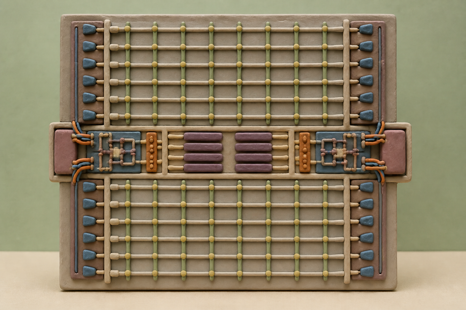
What changes in this design
Without a placement map, a reader might picture storage and supporting electrical parts simply sharing the interior of the memory core.
This record splits the main storage collection into smaller groups, puts support circuits below them, and places reading circuits at one or both column edges. Its central region contains circuits called wordline drivers; their job is not stated. Other device peripheral circuits use another region.
It makes the subject easy to locate: this is about the internal map of a memory core, separating storage from several kinds of electrical support parts. What that placement measures or improves is not stated.
36.9 percent
On June 22, 2025, I came across a number that changed how I read Samsung's memory story. A report citing a market researcher put SK hynix at 36.9 percent of DRAM revenue in the first quarter, ahead of Samsung at 34.4 percent. That reversal mattered because the contest was not only about one high-bandwidth product. It was also about whether a chipmaker could keep fitting more usable memory onto a wafer as ordinary DRAM geometry ran out of room.
That pressure frames how I read US 2026/0253632 A1. Published on August 27, 2026 and assigned to Samsung, it is not a launch announcement. It is a filing about where to put the supporting circuitry in a memory core. Its lineage reaches back to a Korean priority filing of December 29, 2023, so the work in this family predates the market reversal that gives the filing a sharper context today.
Circuitry beneath the cells
Most of us never see the division inside a DRAM chip: dense memory cells occupy the valuable real estate, while the circuitry that selects, reads, and controls them needs its own area. This filing moves part of that circuitry below sub-arrays of cells. Sense amplifiers sit in one or both regions along the columns, wordline drivers occupy a central region, and other device peripheral circuits go elsewhere. The filing shows me a specific spatial arrangement, not evidence that it has solved production.
That distinction matters. A compact arrangement can reclaim area, but it must still connect every layer, carry signals quickly enough, and survive fabrication. The filing makes room beneath the cells rather than beside them. Moving circuitry beneath the cells is, I think, a concrete answer to a real density problem, even before we know whether this particular arrangement will travel from drawings to high-volume wafers.
The 4F2 prototype
Beyond the filing, Samsung demonstrated a 10 nm-class, 16Gb 4F2 DRAM prototype at ISSCC 2026. The reported design combined vertical-channel transistors, cell-over-periphery stacking, and wafer-to-wafer hybrid copper bonding. Compared with a 6F2 cell, its cell size was reported as about 30 percent smaller. This is why the routing choices in the filing matter: a smaller cell only improves a chip if the circuitry around it stops consuming the saved area.
One detailed account of the conference work says Samsung reduced core-circuit area from 17.0 percent of the die to 2.7 percent, while cutting wafer-to-wafer connections from 28.8 million to about 10 million. Those numbers shouldn't, in my view, be treated as proof of a product. They do show the direction of travel: fewer long routes, denser cells, and two wafers joined as one device.
PUC by another name
Naming it CoP doesn't, I think, give Samsung ownership of this basic idea. SK hynix described a roadmap in June 2025 that included bonding circuitry below the cell area. A detailed account of recent conference work treats that Peri-Under-Cell approach and Samsung's Cell-on-Periphery approach as the same fundamental architecture, although the companies use different labels. The shared move is plain: make the cell wafer and the peripheral wafer separately, then bond them.
The idea also has a past outside DRAM. Under-cell peripheral circuitry reached mass production in 128-layer NAND in June 2019, years before these DRAM plans. That mass production is, to me, evidence that the stack itself is not fantasy. But DRAM's speed and retention demands make this a less forgiving migration.
The harder half of the problem
Heat is where the diagram becomes physical. Reports on Samsung's related IEDM work say stacking the cell layer can expose the peripheral transistors beneath it to roughly 550 C, enough to damage conventional materials. Samsung and its research arm presented an amorphous InGaO vertical-channel transistor intended to tolerate that process, with a 100 nm channel and reported threshold shifts below 0.1 eV after a 550 C anneal. Under stress, the reported shift was about -8 mV.
Those are interesting lab numbers, and I won't turn them into a commercial verdict. The 16Gb prototype was reported as not yet verified for mass production, despite testing from -25 C to 95 C with bit failures within repairable limits. RC delay from the stack, plus the floating-body effect that worsens leakage and retention in 4F2 devices, still need attention. US 2026/0253632 A1 maps, as I read it, a credible route to denser DRAM, but the decisive work is making that route cool, reliable, and repeatable at manufacturing scale.
Sources
Reporting for this piece drew on the published filing and the references below.
- Samsung seeks turnaround in HBM
- Samsung Showcases New Technologies for Next-Generation DRAM
- ISSCC 2026 memory, interconnects, and processors deep read
- SK hynix Presents Future DRAM Technology Roadmap at IEEE VLSI 2025
- Micron Steals the Show by Producing Industry's First 176-Layer NAND
- Samsung Unveils Sub-10nm DRAM Breakthrough with InGaO
The record, briefly. US20260253632A1, “Memory Core Circuit Having Cell On Periphery (Cop) Structure And Memory Device Including The Same” A memory core circuit has a memory cell array with sub cell arrays and sub peripheral circuits below them. Sense amplifiers are in one or both column edge regions, wordline drivers are in a central region, and some device peripheral circuits are in another region.
More angles on this
- Memory Array Marks a Pause Worth NoticingAnother reading from the same G11C classification family, static stores.
- A Sideways Reading of Split StaircasesAnother reading from the same G11C classification family, static stores.
- CPC G11C: Static storesThe official classification family this record was filed into, published in the USPTO Cooperative Patent Classification scheme.
- Liquid Cooling Heat Dissipation Device For Multi-Disk Drive System Marks a Pause Worth NoticingAnother reading from the neighbouring G11B classification family, information storage based on relative movement between record carrier and transducer.
- When a Vehicle Notices Something, Who Decides What the Moment Means?Another reading from the wider G06V classification family, image or video recognition or understanding.
Read around this one:Public patent recordUSPTO published figure