Objects
When a Buffer Stops Waiting
Why a new memory patent skips the tiny processors inside DRAM and bets instead on making wasteful data trips fewer.

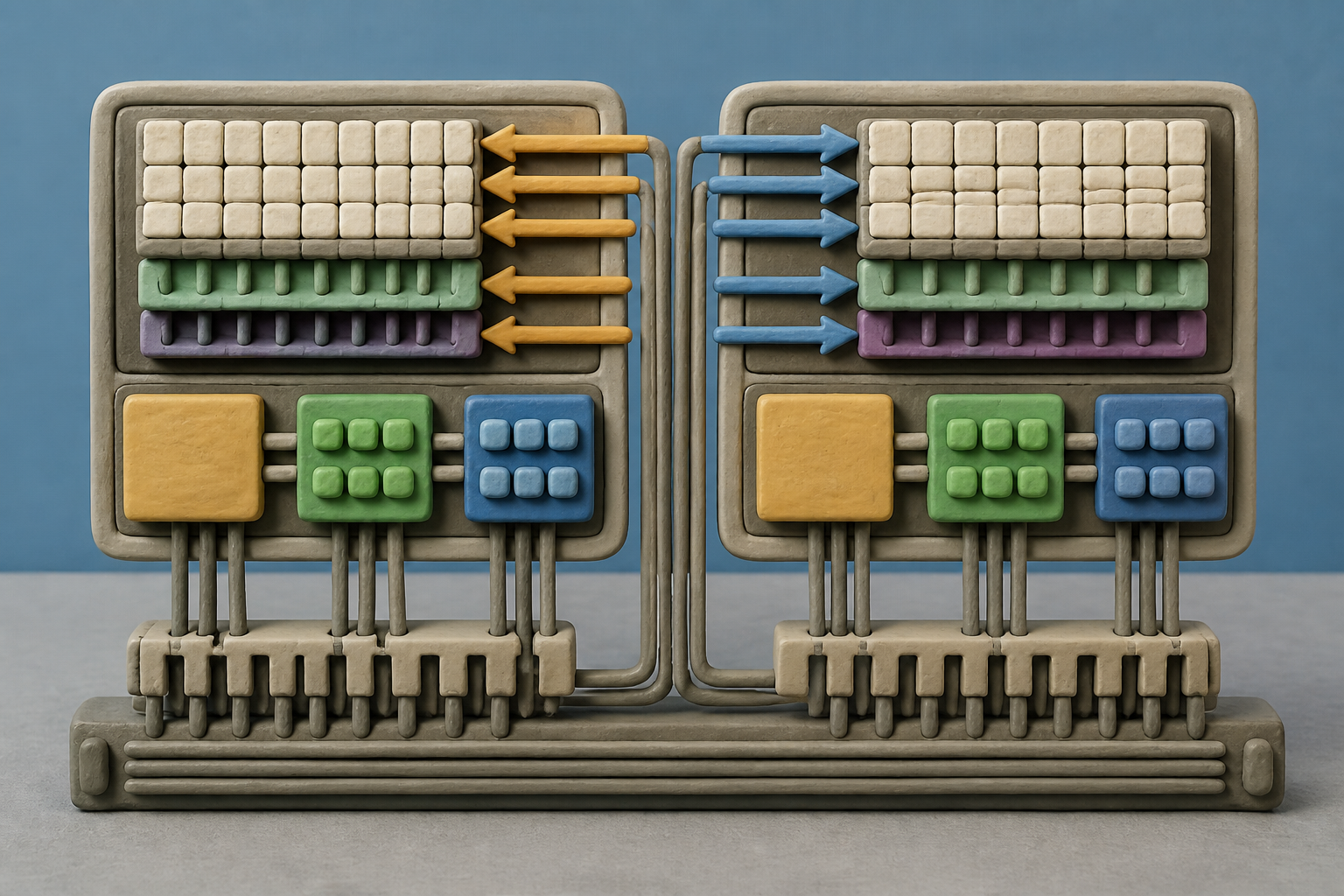
What changes in this design
A reader might picture memory reacting to each requested location as it arrives: receive a request, then immediately read or write there. That is a simple everyday expectation for a component handling requests.
Here, target addresses are first collected in an offset buffer. Rather than acting after every address, the device waits until their number reaches a threshold, then performs a read or write command involving the cell array and stores or transmits the resulting data.
The key detail is the timing: the count of saved locations determines when the memory device moves on to reading or writing. That gives a reader a clear way to understand what this record focuses on, without assuming anything about speed, efficiency, or results.
An August 2021 claim
In August 2021, Samsung reported that its HBM-PIM Aquabolt-XL accelerator card delivered about 2.5 times the system performance and more than 60 percent lower energy use. I can see why. Processing-in-memory puts arithmetic next to data, so fewer bytes make the expensive trip to a processor. The promise was a different division of labor inside the machine.
The reasons it has stayed difficult are clear to me, too. An analyst warned that widespread use remained far off and software rework was the weak point. PIM keeps drawing us back because moving data can dominate a computation, but adding it to DRAM changes more than a benchmark chart.
Sixty-four bytes at a time
The case sharpens in graph processing, where a request may need only four or eight bytes of vertex data while DDR moves a 64-byte burst. The research behind this filing says that mismatch can waste over 90 percent of bytes fetched. The result isn't, to me, a verdict on every program. The mismatch looks like a concrete failure mode for sparse work, where addresses jump around and a cache line arrives mostly empty of value.
The same research group had already published a 2024 precursor on in-memory random scatter-gather and reported a 1.2x to 3.1x speedup on a graph accelerator. That was about 13 months before the later filing's Korean priority date. Its 2025 follow-on paper acknowledges Samsung funding. The connection places the lab result near a serious memory-industry problem, so I mention it, not because it establishes anyone's intent.
The offset buffer
The filing in question is US20260253633A1. It was filed on August 29, 2025, published on August 27, 2026, and assigned to a university research foundation. It claims priority to a Korean application filed on February 26, 2025. Its practical move is narrow. A host supplies target read or write addresses; the device holds them in an offset buffer; and, when their count reaches a threshold, its controller issues a read or write command to the cell array. The resulting data is then stored or transmitted.
Coordination, not computation, is the argument I read in it. The related 2025 paper puts no arithmetic units in DRAM, and its authors cite roughly 50 percent die-area overhead even for fp16-only PIM. Instead, it batches addresses so a memory operation can cover more useful work. In the paper's evaluated setup, the authors report up to 3.28x speedup, a 1.62x geometric-mean speedup, and up to 59.7 percent energy reduction. Those are research results, not promises printed by the patent.
A 2015 head start
The restraint doesn't give the filing an empty field, I don't think. Micron's U.S. patent, granted in 2021 and claiming priority to a 2015 provisional, already describes scatter and gather inside a processing-in-memory device. It uses execution units in individual banks, bins indexes by locality, and sends results over a separate out-of-band bus.
The difference I see is architectural, not magical: the older design performs work in the banks, while this application centers on collecting addresses and triggering cell-array reads or writes at a threshold. These records don't tell me whether the claims overlap in a legally decisive way. I would not call the newer publication a clean break from earlier work.
What the filing is really betting on
HBM4, the high-bandwidth memory standard released in April 2025, came next in my review. JEDEC's release advertises 2 TB/s per stack, a 2,048-bit interface, 32 channels, and capacities up to 64 GB. The release text has an omission: it does not mention processing-in-memory or in-memory compute. The silence doesn't read as a prohibition to me. Still, it suggests that this behavior is not yet presented as a basic standardized feature, even as bandwidth grows enormously.
That omission frames my reading of the filing. The filing is, I think, betting that a smaller intervention can be easier to adopt than putting arithmetic units or small CPUs inside DRAM. It does not promise to turn memory into a general processor. It tries to stop a narrow kind of waste: pulling a full burst for a tiny, scattered piece of data.
Anton Ertl's critique of the old memory-wall story is useful here. Cache misses depend on the data a program touches, not simply on how many instructions it runs, so the wall is not universal. But the graph and sparse workloads in this research are precisely the cases where wasteful movement remains hard to ignore. My view is that the patent's modesty is its strongest idea. It may be more useful to teach memory when to gather than to insist it learn to calculate.
Sources
Reporting for this piece drew on the published filing and the references below.
- US20260253633A1: Memory Device Performing Gather Operation Or Scatter Operation And Method Of Operating The Same
- Memory Device Performing Gather Operation Or Scatter Operation And Method Of Operating The Same - FreePatentsOnline
- A Case for In-Memory Random Scatter-Gather for Fast Graph Processing
- Piccolo: Large-Scale Graph Processing with Fine-Grained In-Memory Scatter-Gather
- Apparatuses and methods for scatter and gather
- JEDEC and Industry Leaders Collaborate to Release JESD270-4 HBM4 Standard
- The Memory Wall Fallacy
The record, briefly. US20260253633A1, “Memory Device Performing Gather Operation Or Scatter Operation And Method Of Operating The Same” A memory device stores host-provided target addresses in an offset buffer and, when their number reaches a threshold, executes a read or write command for the cell array and stores or transmits the resulting data.
More angles on this
- What Holds the SpaceAnother reading from the same G11C classification family, static stores.
- Memory Array Marks a Pause Worth NoticingAnother reading from the same G11C classification family, static stores.
- CPC G11C: Static storesThe official classification family this record was filed into, published in the USPTO Cooperative Patent Classification scheme.
- Liquid Cooling Heat Dissipation Device For Multi-Disk Drive System Marks a Pause Worth NoticingAnother reading from the neighbouring G11B classification family, information storage based on relative movement between record carrier and transducer.
- When a Vehicle Notices Something, Who Decides What the Moment Means?Another reading from the wider G06V classification family, image or video recognition or understanding.
Read around this one:Public patent recordUSPTO published figure